- 您现在的位置:买卖IC网 > PDF目录4106 > MPC755CPX400LE (Freescale Semiconductor)IC MPU PPC 400MHZ 360-FCPBGA PDF资料下载
参数资料
| 型号: | MPC755CPX400LE |
| 厂商: | Freescale Semiconductor |
| 文件页数: | 31/56页 |
| 文件大小: | 0K |
| 描述: | IC MPU PPC 400MHZ 360-FCPBGA |
| 标准包装: | 44 |
| 系列: | MPC7xx |
| 处理器类型: | 32-位 MPC7xx PowerPC |
| 速度: | 400MHz |
| 电压: | 2V |
| 安装类型: | 表面贴装 |
| 封装/外壳: | 360-BBGA,FCCBGA |
| 供应商设备封装: | 360-FCCBGA(25x25) |
| 包装: | 托盘 |
第1页第2页第3页第4页第5页第6页第7页第8页第9页第10页第11页第12页第13页第14页第15页第16页第17页第18页第19页第20页第21页第22页第23页第24页第25页第26页第27页第28页第29页第30页当前第31页第32页第33页第34页第35页第36页第37页第38页第39页第40页第41页第42页第43页第44页第45页第46页第47页第48页第49页第50页第51页第52页第53页第54页第55页第56页
MPC755 RISC Microprocessor Hardware Specifications, Rev. 8
Freescale Semiconductor
37
System Design Information
The MPC755 generates the clock for the external L2 synchronous data SRAMs by dividing the core clock
frequency of the MPC755. The divided-down clock is then phase-adjusted by an on-chip delay-lock-loop
(DLL) circuit and should be routed from the MPC755 to the external RAMs. A separate clock output,
L2SYNC_OUT is sent out half the distance to the SRAMs and then returned as an input to the DLL on pin
L2SYNC_IN so that the rising-edge of the clock as seen at the external RAMs can be aligned to the
clocking of the internal latches in the L2 bus interface.
The core-to-L2 frequency divisor for the L2 PLL is selected through the L2CLK bits of the L2CR register.
Generally, the divisor must be chosen according to the frequency supported by the external RAMs, the
frequency of the MPC755 core, and the phase adjustment range that the L2 DLL supports. Table 17 shows
various example L2 clock frequencies that can be obtained for a given set of core frequencies. The
minimum L2 frequency target is 80 MHz.
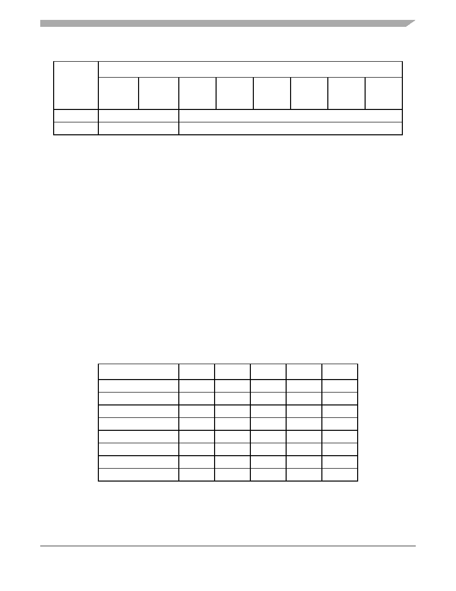
0011
PLL off/bypass
PLL off, SYSCLK clocks core circuitry directly, 1x bus-to-core implied
1111
PLL off
PLL off, no core clocking occurs
Notes:
1. PLL_CFG[0:3] settings not listed are reserved.
2. The sample bus-to-core frequencies shown are for reference only. Some PLL configurations may select bus, core,
or VCO frequencies which are not useful, not supported, or not tested for by the MPC755; see Section 4.2.1, “Clock
AC Specifications,” for valid SYSCLK, core, and VCO frequencies.
3. In PLL-bypass mode, the SYSCLK input signal clocks the internal processor directly, the PLL is disabled, and the
bus mode is set for 1:1 mode operation. This mode is intended for factory use and emulator tool use only.
Note: The AC timing specifications given in this document do not apply in PLL-bypass mode.
4. In PLL off mode, no clocking occurs inside the MPC755 regardless of the SYSCLK input.
Table 17. Sample Core-to-L2 Frequencies
Core Frequency (MHz)
÷1
÷1.5
÷2
÷2.5
÷3
250
166
125
100
83
266
177
133
106
89
275
183
138
110
92
300
200
150
120
100
325
217
163
130
108
333
222
167
133
111
350
233
175
140
117
366
244
183
146
122
Table 16. MPC755 Microprocessor PLL Configuration Example for 400 MHz Parts (continued)
PLL_CFG
[0:3]
Example Bus-to-Core Frequency in MHz (VCO Frequency in MHz)
Bus-to-
Core
Multiplier
Core-to-
VCO
Multiplier
Bus
33 MHz
Bus
50 MHz
Bus
66 MHz
Bus
75 MHz
Bus
80 MHz
Bus
100 MHz
相关PDF资料 |
PDF描述 |
|---|---|
| IDT71V67803S133BGG8 | IC SRAM 9MBIT 133MHZ 119BGA |
| IDT71V67803S133BG8 | IC SRAM 9MBIT 133MHZ 119BGA |
| MPC862PZQ100B | IC MPU POWERQUICC 100MHZ 357PBGA |
| IDT71V67703S85BG8 | IC SRAM 9MBIT 85NS 119BGA |
| MPC8349EVVALFB | IC MPU POWERQUICC II 672-TBGA |
相关代理商/技术参数 |
参数描述 |
|---|---|
| MPC755CPX400LE | 制造商:Freescale Semiconductor 功能描述:IC 32BIT MPU 400MHZ BGA-360 |
| MPC755CPX400LER2 | 功能描述:微处理器 - MPU GF RV2.8360PBGA 4A105C RoHS:否 制造商:Atmel 处理器系列:SAMA5D31 核心:ARM Cortex A5 数据总线宽度:32 bit 最大时钟频率:536 MHz 程序存储器大小:32 KB 数据 RAM 大小:128 KB 接口类型:CAN, Ethernet, LIN, SPI,TWI, UART, USB 工作电源电压:1.8 V to 3.3 V 最大工作温度:+ 85 C 安装风格:SMD/SMT 封装 / 箱体:FBGA-324 |
| MPC755CRX350LE | 功能描述:微处理器 - MPU 360CBGA,RV2.8,6W RoHS:否 制造商:Atmel 处理器系列:SAMA5D31 核心:ARM Cortex A5 数据总线宽度:32 bit 最大时钟频率:536 MHz 程序存储器大小:32 KB 数据 RAM 大小:128 KB 接口类型:CAN, Ethernet, LIN, SPI,TWI, UART, USB 工作电源电压:1.8 V to 3.3 V 最大工作温度:+ 85 C 安装风格:SMD/SMT 封装 / 箱体:FBGA-324 |
| MPC755CRX350TE | 功能描述:微处理器 - MPU 360CBGA,RV2.8, RoHS:否 制造商:Atmel 处理器系列:SAMA5D31 核心:ARM Cortex A5 数据总线宽度:32 bit 最大时钟频率:536 MHz 程序存储器大小:32 KB 数据 RAM 大小:128 KB 接口类型:CAN, Ethernet, LIN, SPI,TWI, UART, USB 工作电源电压:1.8 V to 3.3 V 最大工作温度:+ 85 C 安装风格:SMD/SMT 封装 / 箱体:FBGA-324 |
| MPC755CRX400LE | 功能描述:微处理器 - MPU GF RV2.84A105C 360CBGA RoHS:否 制造商:Atmel 处理器系列:SAMA5D31 核心:ARM Cortex A5 数据总线宽度:32 bit 最大时钟频率:536 MHz 程序存储器大小:32 KB 数据 RAM 大小:128 KB 接口类型:CAN, Ethernet, LIN, SPI,TWI, UART, USB 工作电源电压:1.8 V to 3.3 V 最大工作温度:+ 85 C 安装风格:SMD/SMT 封装 / 箱体:FBGA-324 |
发布紧急采购,3分钟左右您将得到回复。