- 您现在的位置:买卖IC网 > PDF目录98027 > MPC8240LZU250X (MOTOROLA INC) 32-BIT, 250 MHz, RISC PROCESSOR, PBGA352 PDF资料下载
参数资料
| 型号: | MPC8240LZU250X |
| 厂商: | MOTOROLA INC |
| 元件分类: | 微控制器/微处理器 |
| 英文描述: | 32-BIT, 250 MHz, RISC PROCESSOR, PBGA352 |
| 封装: | TBGA-352 |
| 文件页数: | 11/52页 |
| 文件大小: | 542K |
| 代理商: | MPC8240LZU250X |
第1页第2页第3页第4页第5页第6页第7页第8页第9页第10页当前第11页第12页第13页第14页第15页第16页第17页第18页第19页第20页第21页第22页第23页第24页第25页第26页第27页第28页第29页第30页第31页第32页第33页第34页第35页第36页第37页第38页第39页第40页第41页第42页第43页第44页第45页第46页第47页第48页第49页第50页第51页第52页
MPC8240 (rev0.5) Hardware Specifications
19
PRELIMINARY—SUBJECT TO CHANGE WITHOUT NOTICE
Electrical and Thermal Characteristics
Notes:
1
All memory and related interface output signal specications are specied from the VM = 1.4 V of the ris-
ing edge of the memory bus clock, SDRAM_SYNC_IN to the TTL level (0.8 or 2.0 V) of the signal in
question. SDRAM_SYNC_IN is the same as PCI_SYNC_IN in 1:1 mode, but is twice the frequency in
2:1 mode (processor/memory bus clock rising edges occur on every rising and falling edge of
PCI_SYNC_IN). See Figure 6.
2
All PCI signals are measured from OVdd/2 of the rising edge of PCI_SYNC_IN to 0.285*OVdd or
0.615*OVdd of the signal in question for 3.3 V PCI signaling levels. See Figure 7.
3
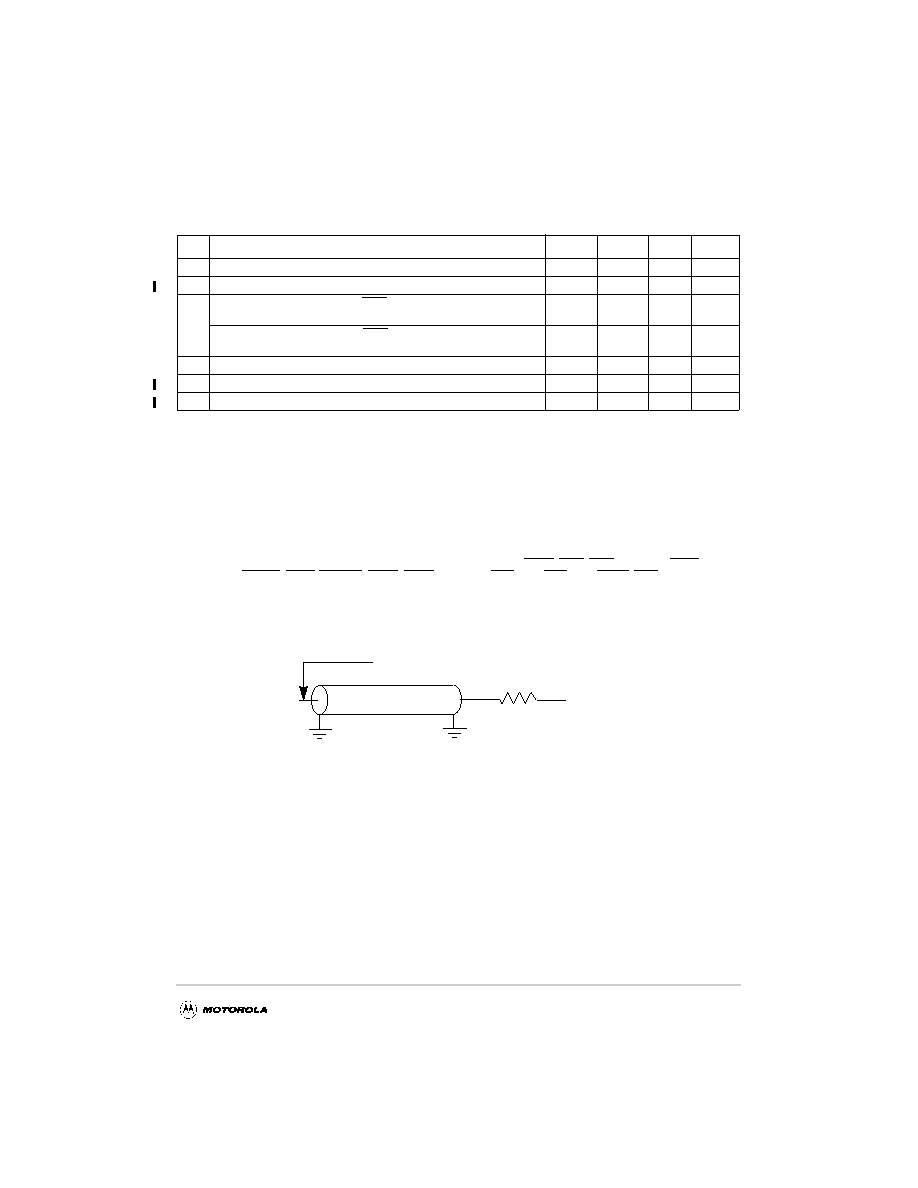
All output timings assume a purely resistive 50 ohm load (See Figure 9). Output timings are measured at
the pin; time-of-ight delays must be added for trace lengths, vias, and connectors in the system.
4
PCI Bussed signals are composed of the following signals: LOCK, IRDY, C/BE[0–3], PAR, TRDY,
FRAME, STOP, DEVSEL, PERR, SERR, AD[0–31], REQ[4–0], GNT[4–0], IDSEL, INTA.
5
PCI hold times can be varied, see 1.4.3.3.1 “PCI Signal Output Hold Timing” section for information on
programmable PCI output hold times. The values shown for item 13a are for PCI compliance.
6
These specications are for the default driver strengths indicated in Table 4.
.
Figure 9. AC Test Load for the MPC8240
12c
SDRAM_SYNC_IN to Output Valid (For All Others)
—
7.0
ns
1
12d
SDRAM_SYNC_IN to Output Valid (For I2C)
—
5.0
ns
1
13a
Output Hold, 66 MHz PCI, with MCP and CKE pulled-down to logic 0
states. See Table 11.
1.0
—
ns
2,4,5
Output Hold, 33 MHz PCI, with MCP in the default logic 1 state and
CKE pulled-down to logic 0 state. See Table 11.
2.0
—
ns
2,4,5
13b
Output Hold (All Others)
0
—
ns
1
14a
PCI_SYNC_IN to Output High Impedance (For PCI)
—
14.0
ns
2,4
14b
SDRAM_SYNC_IN to Output High Impedance (For All Others)
—
4.0
ns
1
Table 10. Output AC Timing Specifications (Continued)
At recommended operating conditions (See Table 2) with GVdd = 3.3 V ± 5% and LVdd = 3.3 V ± 5%
Num
Characteristic3,6
Min
Max
Units
Notes
OUTPUT
Z0 = 50
OVdd/2
RL = 50
PIN
Output measurements are made at the device pin.
相关PDF资料 |
PDF描述 |
|---|---|
| MPC8240RZU266X | 32-BIT, 266 MHz, RISC PROCESSOR, PBGA352 |
| MPC8245LZU300X | 32-BIT, 300 MHz, RISC PROCESSOR, PBGA352 |
| MPC8245LZU350X | 32-BIT, 350 MHz, RISC PROCESSOR, PBGA352 |
| MPC8270CVVQLDA | 32-BIT, 333 MHz, RISC PROCESSOR, PBGA480 |
| MPC8270CZUQLDA | 32-BIT, 333 MHz, RISC PROCESSOR, PBGA480 |
相关代理商/技术参数 |
参数描述 |
|---|---|
| MPC8241 | 制造商:FREESCALE 制造商全称:Freescale Semiconductor, Inc 功能描述:Intergrated Processor Hardware Specifications |
| MPC8241EC | 制造商:FREESCALE 制造商全称:Freescale Semiconductor, Inc 功能描述:MPC8241 Integrated Processor Hardware Specifications |
| MPC8241LVR166D | 功能描述:微处理器 - MPU INTEGRATED HOST PROC RoHS:否 制造商:Atmel 处理器系列:SAMA5D31 核心:ARM Cortex A5 数据总线宽度:32 bit 最大时钟频率:536 MHz 程序存储器大小:32 KB 数据 RAM 大小:128 KB 接口类型:CAN, Ethernet, LIN, SPI,TWI, UART, USB 工作电源电压:1.8 V to 3.3 V 最大工作温度:+ 85 C 安装风格:SMD/SMT 封装 / 箱体:FBGA-324 |
| MPC8241LVR200D | 功能描述:微处理器 - MPU INTEGRATED HOST PROC RoHS:否 制造商:Atmel 处理器系列:SAMA5D31 核心:ARM Cortex A5 数据总线宽度:32 bit 最大时钟频率:536 MHz 程序存储器大小:32 KB 数据 RAM 大小:128 KB 接口类型:CAN, Ethernet, LIN, SPI,TWI, UART, USB 工作电源电压:1.8 V to 3.3 V 最大工作温度:+ 85 C 安装风格:SMD/SMT 封装 / 箱体:FBGA-324 |
| MPC8241LVR266D | 功能描述:微处理器 - MPU INTEGRATED HOST PROC RoHS:否 制造商:Atmel 处理器系列:SAMA5D31 核心:ARM Cortex A5 数据总线宽度:32 bit 最大时钟频率:536 MHz 程序存储器大小:32 KB 数据 RAM 大小:128 KB 接口类型:CAN, Ethernet, LIN, SPI,TWI, UART, USB 工作电源电压:1.8 V to 3.3 V 最大工作温度:+ 85 C 安装风格:SMD/SMT 封装 / 箱体:FBGA-324 |
发布紧急采购,3分钟左右您将得到回复。