- 您现在的位置:买卖IC网 > PDF目录98027 > MPC8240LZU250X (MOTOROLA INC) 32-BIT, 250 MHz, RISC PROCESSOR, PBGA352 PDF资料下载
参数资料
| 型号: | MPC8240LZU250X |
| 厂商: | MOTOROLA INC |
| 元件分类: | 微控制器/微处理器 |
| 英文描述: | 32-BIT, 250 MHz, RISC PROCESSOR, PBGA352 |
| 封装: | TBGA-352 |
| 文件页数: | 33/52页 |
| 文件大小: | 542K |
| 代理商: | MPC8240LZU250X |
第1页第2页第3页第4页第5页第6页第7页第8页第9页第10页第11页第12页第13页第14页第15页第16页第17页第18页第19页第20页第21页第22页第23页第24页第25页第26页第27页第28页第29页第30页第31页第32页当前第33页第34页第35页第36页第37页第38页第39页第40页第41页第42页第43页第44页第45页第46页第47页第48页第49页第50页第51页第52页
MPC8240 (rev0.5) Hardware Specifications
39
PRELIMINARY—SUBJECT TO CHANGE WITHOUT NOTICE
System Design Information
power plane is not loaded as much as the OVdd/GVdd power plane and thus Vdd/AVdd/AVdd2/LAVdd
ramps at a faster rate than OVdd/GVdd.
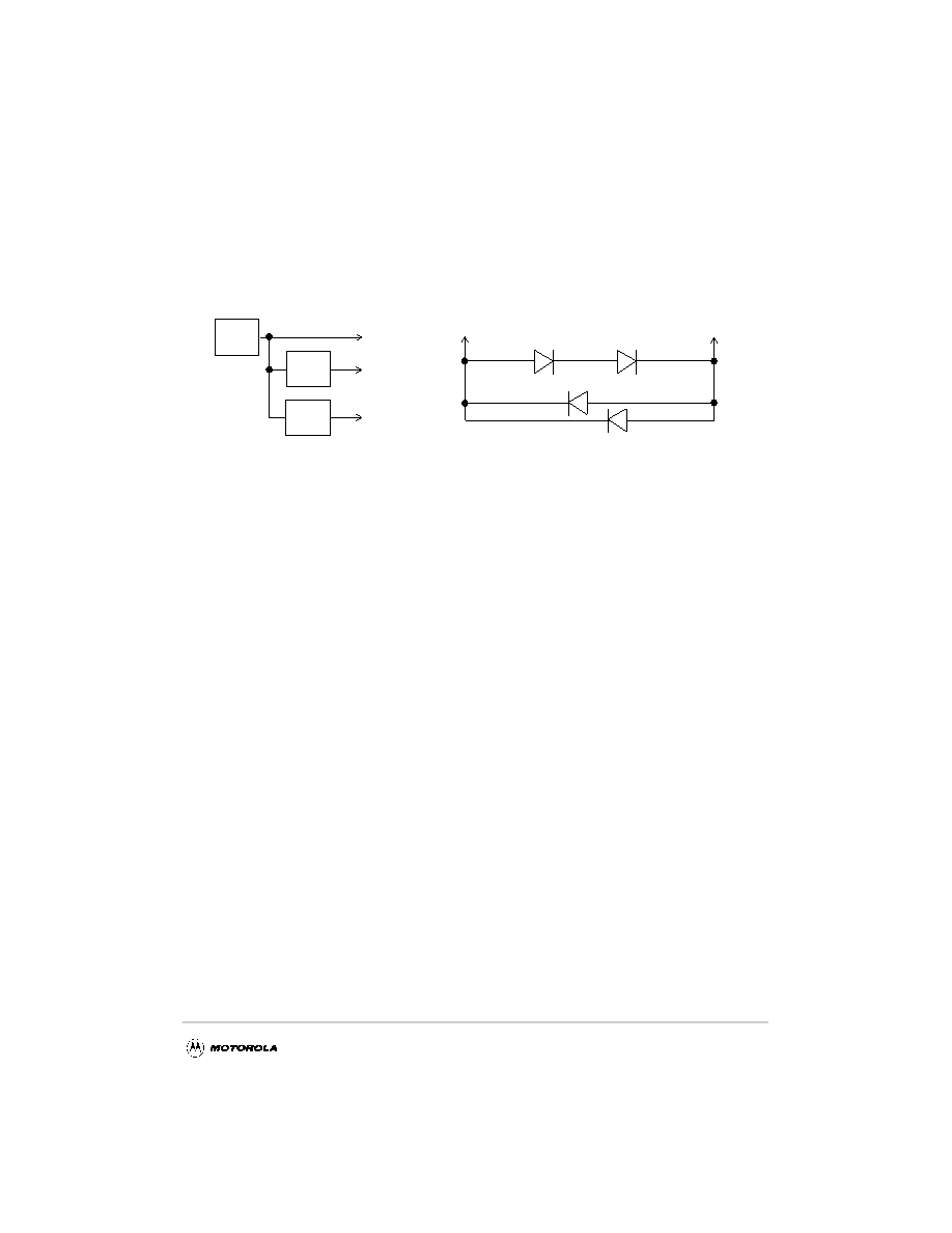
If the system power supply design does not control the voltage sequencing, the circuit of Figure 23 can be
added to meet these requirements. The MUR420 diodes of Figure 23 control the maximum potential
difference between the 3.3 bus and internal voltages on power-up and the 1N5820 Schottky diodes regulate
the maximum potential difference on power-down.
Figure 23. Example Voltage Sequencing Circuits
1.7.3 Power Supply Sizing
The power consumption numbers provided in Table 5 do not reect power from the OVdd and GVdd power
supplies which are non-negligible for the MPC8240. In typical application measurements, the OVdd power
ranged from 200 to 600 mW and the GVdd power ranged from 300 to 900 mW. The ranges’ low end power
numbers were results of the MPC8240 performing cache resident integer operations at the slowest
frequency combination of 33:66:166 (PCI:Mem:CPU) MHz. The OVdd high end range’s value resulted
from the MPC8240 performing continuous ushes of cache lines with alternating ones and zeroes to PCI
memory. The GVdd high end range’s value resulted from the MPC8240 operating at the fastest frequency
combination of 66:100:250 (PCI:Mem:CPU) MHz and performing continuous ushes of cache lines with
alternating ones and zeroes on 64 bit boundaries to local memory.
1.7.4 Decoupling Recommendations
Due to the MPC8240’s dynamic power management feature, large address and data buses, and high
operating frequencies, the MPC8240 can generate transient power surges and high frequency noise in its
power supply, especially while driving large capacitive loads. This noise must be prevented from reaching
other components in the MPC8240 system, and the MPC8240 itself requires a clean, tightly regulated
source of power. Therefore, it is recommended that the system designer place at least one decoupling
capacitor at each Vdd, OVdd, GVdd, and LVdd pin of the MPC8240. It is also recommended that these
decoupling capacitors receive their power from separate Vdd, OVdd, GVdd, and GND power planes in the
PCB, utilizing short traces to minimize inductance. These capacitors should have a value of 0.1 F. Only
ceramic SMT (surface mount technology) capacitors should be used to minimize lead inductance,
preferably 0508 or 0603, oriented such that connections are made along the length of the part.
In addition, it is recommended that there be several bulk storage capacitors distributed around the PCB,
feeding the Vdd, OVdd, GVdd, and LVdd planes, to enable quick recharging of the smaller chip capacitors.
These bulk capacitors should have a low ESR (equivalent series resistance) rating to ensure the quick
response time necessary. They should also be connected to the power and ground planes through two vias
to minimize inductance. Suggested bulk capacitors—100–330 F (AVX TPS tantalum or Sanyo OSCON).
3.3V
MUR420
1N5820
MUR420
1N5820
2.5V
+3.3V
+2.5V
Source
+5V
Source
5V
3.3V
2.5V
相关PDF资料 |
PDF描述 |
|---|---|
| MPC8240RZU266X | 32-BIT, 266 MHz, RISC PROCESSOR, PBGA352 |
| MPC8245LZU300X | 32-BIT, 300 MHz, RISC PROCESSOR, PBGA352 |
| MPC8245LZU350X | 32-BIT, 350 MHz, RISC PROCESSOR, PBGA352 |
| MPC8270CVVQLDA | 32-BIT, 333 MHz, RISC PROCESSOR, PBGA480 |
| MPC8270CZUQLDA | 32-BIT, 333 MHz, RISC PROCESSOR, PBGA480 |
相关代理商/技术参数 |
参数描述 |
|---|---|
| MPC8241 | 制造商:FREESCALE 制造商全称:Freescale Semiconductor, Inc 功能描述:Intergrated Processor Hardware Specifications |
| MPC8241EC | 制造商:FREESCALE 制造商全称:Freescale Semiconductor, Inc 功能描述:MPC8241 Integrated Processor Hardware Specifications |
| MPC8241LVR166D | 功能描述:微处理器 - MPU INTEGRATED HOST PROC RoHS:否 制造商:Atmel 处理器系列:SAMA5D31 核心:ARM Cortex A5 数据总线宽度:32 bit 最大时钟频率:536 MHz 程序存储器大小:32 KB 数据 RAM 大小:128 KB 接口类型:CAN, Ethernet, LIN, SPI,TWI, UART, USB 工作电源电压:1.8 V to 3.3 V 最大工作温度:+ 85 C 安装风格:SMD/SMT 封装 / 箱体:FBGA-324 |
| MPC8241LVR200D | 功能描述:微处理器 - MPU INTEGRATED HOST PROC RoHS:否 制造商:Atmel 处理器系列:SAMA5D31 核心:ARM Cortex A5 数据总线宽度:32 bit 最大时钟频率:536 MHz 程序存储器大小:32 KB 数据 RAM 大小:128 KB 接口类型:CAN, Ethernet, LIN, SPI,TWI, UART, USB 工作电源电压:1.8 V to 3.3 V 最大工作温度:+ 85 C 安装风格:SMD/SMT 封装 / 箱体:FBGA-324 |
| MPC8241LVR266D | 功能描述:微处理器 - MPU INTEGRATED HOST PROC RoHS:否 制造商:Atmel 处理器系列:SAMA5D31 核心:ARM Cortex A5 数据总线宽度:32 bit 最大时钟频率:536 MHz 程序存储器大小:32 KB 数据 RAM 大小:128 KB 接口类型:CAN, Ethernet, LIN, SPI,TWI, UART, USB 工作电源电压:1.8 V to 3.3 V 最大工作温度:+ 85 C 安装风格:SMD/SMT 封装 / 箱体:FBGA-324 |
发布紧急采购,3分钟左右您将得到回复。