- 您现在的位置:买卖IC网 > PDF目录17033 > MPC8308-KIT (Freescale Semiconductor)KIT EVALUATION FOR MPC830X PDF资料下载
参数资料
| 型号: | MPC8308-KIT |
| 厂商: | Freescale Semiconductor |
| 文件页数: | 23/83页 |
| 文件大小: | 0K |
| 描述: | KIT EVALUATION FOR MPC830X |
| 标准包装: | 1 |
| 系列: | PowerQUICC II™ PRO |
| 类型: | MPU |
| 适用于相关产品: | MPC8308 |
| 所含物品: | 板,线缆,CD,电源 |
第1页第2页第3页第4页第5页第6页第7页第8页第9页第10页第11页第12页第13页第14页第15页第16页第17页第18页第19页第20页第21页第22页当前第23页第24页第25页第26页第27页第28页第29页第30页第31页第32页第33页第34页第35页第36页第37页第38页第39页第40页第41页第42页第43页第44页第45页第46页第47页第48页第49页第50页第51页第52页第53页第54页第55页第56页第57页第58页第59页第60页第61页第62页第63页第64页第65页第66页第67页第68页第69页第70页第71页第72页第73页第74页第75页第76页第77页第78页第79页第80页第81页第82页第83页
MPC8308 PowerQUICC II Pro Processor Hardware Specification, Rev. 3
Freescale Semiconductor
3
Electrical Characteristics
2.1.1
Absolute Maximum Ratings
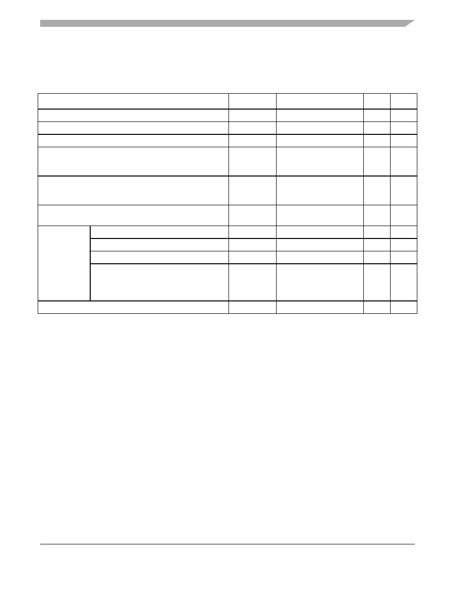
This table lists the absolute maximum ratings.
2.1.2
Power Supply Voltage Specification
This table provides the recommended operating conditions for the device. Note that the values in this table
are the recommended and tested operating conditions. Proper device operation outside of these conditions
is not guaranteed.
Table 1. Absolute Maximum Ratings1
Characteristic
Symbol
Max Value
Unit
Notes
Core supply voltage
VDD
–0.3 to 1.26
V
—
PLL supply voltage
AVDD1, AVDD2
–0.3 to 1.26
V
—
DDR2 DRAM I/O voltage
GVDD
–0.3 to 1.9
V
—
Local bus, DUART, system control and power management,
eSDHC, I2C, USB, Interrupt, Ethernet management, SPI,
Miscellaneous and JTAG I/O voltage
NVDD
–0.3 to 3.6
V
7
SerDes PHY
XCOREVDD,
XPADVDD,
SDAVDD
–0.3 to 1.26
V
—
eTSEC I/O Voltage
LVDD1, LVDD2
–0.3 to 2.75 or
–0.3 to 3.6
V6, 8
Input voltage
DDR2 DRAM signals
MVIN
–0.3 to (GVDD + 0.3)
V
2, 5
DDR2 DRAM reference
MVREF
–0.3 to (GVDD + 0.3)
V
2, 5
eTSEC
LVIN
–0.3 to (LVDD + 0.3)
V
4, 5,8
Local bus, DUART, system control and power
management, eSDHC, I2C, Interrupt,
Ethernet management, SPI, Miscellaneous
and JTAG I/O voltage
OVIN
–0.3 to (NVDD + 0.3)
V
3, 5,7
Storage temperature range
TSTG
–55 to 150
C—
Notes:
1. Functional and tested operating conditions are given in Table 2. Absolute maximum ratings are stress ratings only, and
functional operation at the maximums is not guaranteed. Stresses beyond those listed may affect device reliability or cause
permanent damage to the device.
2. Caution: MVIN must not exceed GVDD by more than 0.3 V. This limit may be exceeded for a maximum of 20 ms during
power-on reset and power-down sequences.
3. Caution: OVIN must not exceed NVDD by more than 0.3 V. This limit may be exceeded for a maximum of 20 ms during
power-on reset and power-down sequences.
4. Caution: LVIN must not exceed LVDD by more than 0.3 V. This limit may be exceeded for a maximum of 20 ms during power-on
reset and power-down sequences.
5. (M, L, O)VIN and MVREF may overshoot/undershoot to a voltage and for a maximum duration as shown in Figure 2
6. The max value of supply voltage should be selected based on the RGMII mode. The lower range applies to RGMII mode.
7. NVDD here refers to NVDDA, NVDDB,NVDDG, NVDDH, NVDDJ, NVDDP_K from the ball map.
8. LVDD1 here refers to NVDDC and LVDD2 refers to NVDDF from the ball map
相关PDF资料 |
PDF描述 |
|---|---|
| EBA22DTMH | CONN EDGECARD 44POS R/A .125 SLD |
| EBA22DTMD | CONN EDGECARD 44POS R/A .125 SLD |
| EBM36DCSN | CONN EDGECARD 72POS DIP .156 SLD |
| EBA22DTBN | CONN EDGECARD 44POS R/A .125 SLD |
| EBM36DCSH | CONN EDGECARD 72POS DIP .156 SLD |
相关代理商/技术参数 |
参数描述 |
|---|---|
| MPC8308-NSG | 功能描述:开发板和工具包 - 其他处理器 MPC8308-NSG RoHS:否 制造商:Freescale Semiconductor 产品:Development Systems 工具用于评估:P3041 核心:e500mc 接口类型:I2C, SPI, USB 工作电源电压: |
| MPC8308-NSG | 制造商:Freescale Semiconductor 功能描述:MPC8308-NSG*NIC* |
| MPC8308-RDB | 功能描述:开发板和工具包 - 其他处理器 Refer. Board MPC8308 RoHS:否 制造商:Freescale Semiconductor 产品:Development Systems 工具用于评估:P3041 核心:e500mc 接口类型:I2C, SPI, USB 工作电源电压: |
| MPC8308-RDB-PROMO | 制造商:Freescale 功能描述:Motherboards MPC8308 PowerQuicc II DDR2 10Mbps/100Mbps/1000Mbps Linux Kernel |
| MPC8308-SOM | 功能描述:开发板和工具包 - 其他处理器 For MPC8308 Ethernet USB 32bit RoHS:否 制造商:Freescale Semiconductor 产品:Development Systems 工具用于评估:P3041 核心:e500mc 接口类型:I2C, SPI, USB 工作电源电压: |
发布紧急采购,3分钟左右您将得到回复。