- 您现在的位置:买卖IC网 > PDF目录17033 > MPC8308-KIT (Freescale Semiconductor)KIT EVALUATION FOR MPC830X PDF资料下载
参数资料
| 型号: | MPC8308-KIT |
| 厂商: | Freescale Semiconductor |
| 文件页数: | 75/83页 |
| 文件大小: | 0K |
| 描述: | KIT EVALUATION FOR MPC830X |
| 标准包装: | 1 |
| 系列: | PowerQUICC II™ PRO |
| 类型: | MPU |
| 适用于相关产品: | MPC8308 |
| 所含物品: | 板,线缆,CD,电源 |
第1页第2页第3页第4页第5页第6页第7页第8页第9页第10页第11页第12页第13页第14页第15页第16页第17页第18页第19页第20页第21页第22页第23页第24页第25页第26页第27页第28页第29页第30页第31页第32页第33页第34页第35页第36页第37页第38页第39页第40页第41页第42页第43页第44页第45页第46页第47页第48页第49页第50页第51页第52页第53页第54页第55页第56页第57页第58页第59页第60页第61页第62页第63页第64页第65页第66页第67页第68页第69页第70页第71页第72页第73页第74页当前第75页第76页第77页第78页第79页第80页第81页第82页第83页
MPC8308 PowerQUICC II Pro Processor Hardware Specification, Rev. 3
Freescale Semiconductor
77
System Design Information
23 System Design Information
This section provides electrical and thermal design recommendations for successful application of the
device
23.1
System Clocking
The device includes two PLLs.
1. The platform PLL generates the platform clock from the externally supplied SYS_CLK_IN input.
The frequency ratio between the platform and SYS_CLK_IN is selected using the platform PLL
ratio configuration bits as described in Section 21.2, “System PLL Configuration.”
2. The e300 core PLL generates the core clock as a slave to the platform clock. The frequency ratio
between the e300 core clock and the platform clock is selected using the e300 PLL ratio
configuration bits as described in Section 21.3, “Core PLL Configuration.”
23.2
PLL Power Supply Filtering
Each of the PLLs listed above is provided with power through independent power supply pins (AVDD1 for
core PLL and AVDD2 for the platform PLL). The AVDD level should always be equivalent to VDD, and
preferably these voltages are derived directly from VDD through a low pass filter scheme such as the
following.
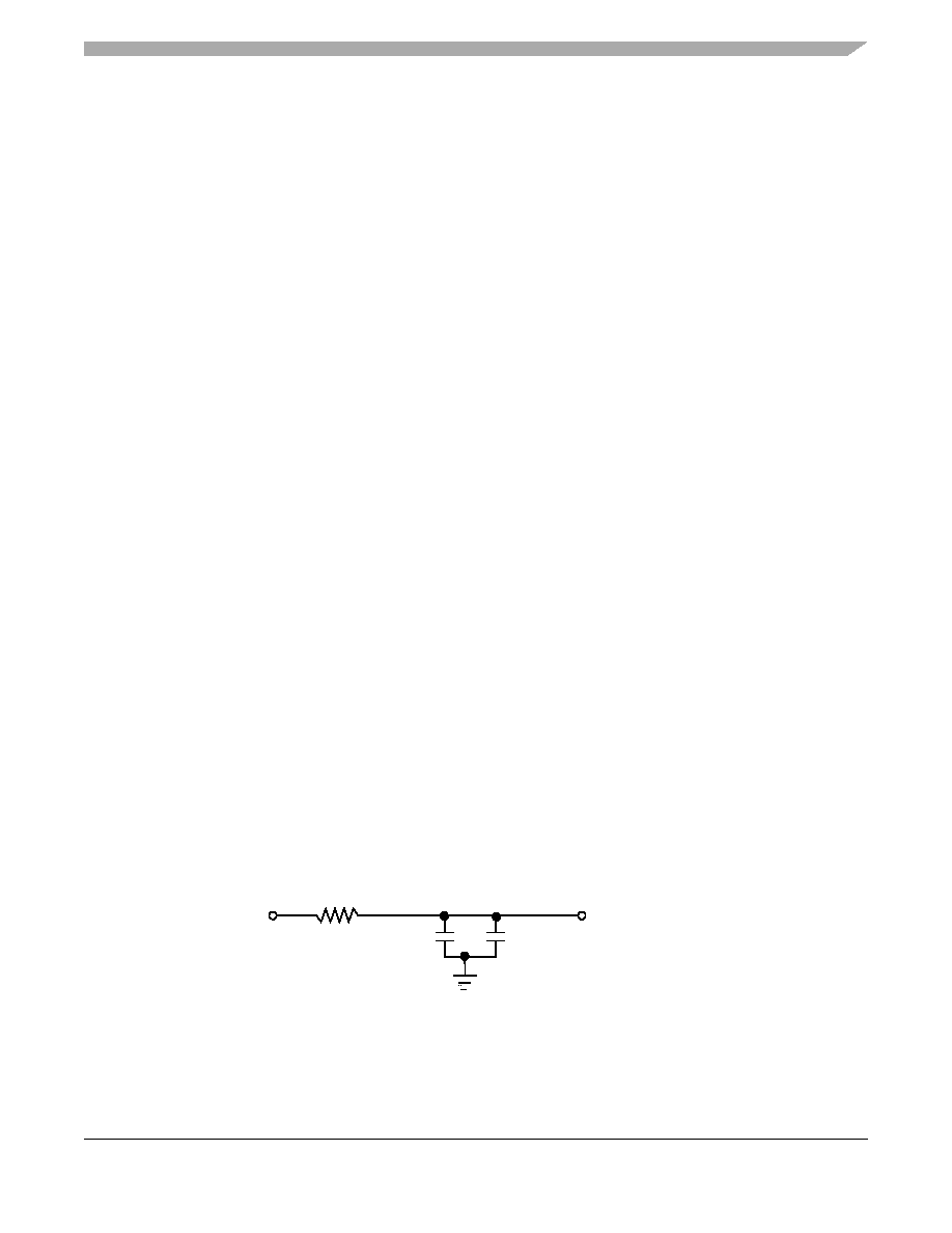
There are a number of ways to reliably provide power to the PLLs, but the recommended solution is to
provide independent filter circuits as illustrated in Figure 54, one to each of the two AVDD pins. By
providing independent filters to each PLL the opportunity to cause noise injection from one PLL to the
other is reduced.
This circuit is intended to filter noise in the PLLs’ resonant frequency range from a 500 kHz to 10 MHz
range. It should be built with surface mount capacitors with minimum effective series inductance (ESL).
Consistent with the recommendations of Dr. Howard Johnson in High Speed Digital Design: A Handbook
of Black Magic (Prentice Hall, 1993), multiple small capacitors of equal value are recommended over a
single large value capacitor.
Each circuit should be placed as close as possible to the specific AVDD pin being supplied to minimize
noise coupled from nearby circuits. It should be possible to route directly from the capacitors to the AVDD
pin, which is on the periphery of package, without the inductance of vias.
This figure shows the PLL power supply filter circuits.
Figure 54. PLL Power Supply Filter Circuit
VDD
AVDD1 and AVDD2
2.2 F
Low ESL Surface Mount Capacitors
10
相关PDF资料 |
PDF描述 |
|---|---|
| EBA22DTMH | CONN EDGECARD 44POS R/A .125 SLD |
| EBA22DTMD | CONN EDGECARD 44POS R/A .125 SLD |
| EBM36DCSN | CONN EDGECARD 72POS DIP .156 SLD |
| EBA22DTBN | CONN EDGECARD 44POS R/A .125 SLD |
| EBM36DCSH | CONN EDGECARD 72POS DIP .156 SLD |
相关代理商/技术参数 |
参数描述 |
|---|---|
| MPC8308-NSG | 功能描述:开发板和工具包 - 其他处理器 MPC8308-NSG RoHS:否 制造商:Freescale Semiconductor 产品:Development Systems 工具用于评估:P3041 核心:e500mc 接口类型:I2C, SPI, USB 工作电源电压: |
| MPC8308-NSG | 制造商:Freescale Semiconductor 功能描述:MPC8308-NSG*NIC* |
| MPC8308-RDB | 功能描述:开发板和工具包 - 其他处理器 Refer. Board MPC8308 RoHS:否 制造商:Freescale Semiconductor 产品:Development Systems 工具用于评估:P3041 核心:e500mc 接口类型:I2C, SPI, USB 工作电源电压: |
| MPC8308-RDB-PROMO | 制造商:Freescale 功能描述:Motherboards MPC8308 PowerQuicc II DDR2 10Mbps/100Mbps/1000Mbps Linux Kernel |
| MPC8308-SOM | 功能描述:开发板和工具包 - 其他处理器 For MPC8308 Ethernet USB 32bit RoHS:否 制造商:Freescale Semiconductor 产品:Development Systems 工具用于评估:P3041 核心:e500mc 接口类型:I2C, SPI, USB 工作电源电压: |
发布紧急采购,3分钟左右您将得到回复。