- 您现在的位置:买卖IC网 > PDF目录17033 > MPC8308-KIT (Freescale Semiconductor)KIT EVALUATION FOR MPC830X PDF资料下载
参数资料
| 型号: | MPC8308-KIT |
| 厂商: | Freescale Semiconductor |
| 文件页数: | 47/83页 |
| 文件大小: | 0K |
| 描述: | KIT EVALUATION FOR MPC830X |
| 标准包装: | 1 |
| 系列: | PowerQUICC II™ PRO |
| 类型: | MPU |
| 适用于相关产品: | MPC8308 |
| 所含物品: | 板,线缆,CD,电源 |
第1页第2页第3页第4页第5页第6页第7页第8页第9页第10页第11页第12页第13页第14页第15页第16页第17页第18页第19页第20页第21页第22页第23页第24页第25页第26页第27页第28页第29页第30页第31页第32页第33页第34页第35页第36页第37页第38页第39页第40页第41页第42页第43页第44页第45页第46页当前第47页第48页第49页第50页第51页第52页第53页第54页第55页第56页第57页第58页第59页第60页第61页第62页第63页第64页第65页第66页第67页第68页第69页第70页第71页第72页第73页第74页第75页第76页第77页第78页第79页第80页第81页第82页第83页
MPC8308 PowerQUICC II Pro Processor Hardware Specification, Rev. 3
Freescale Semiconductor
51
JTAG
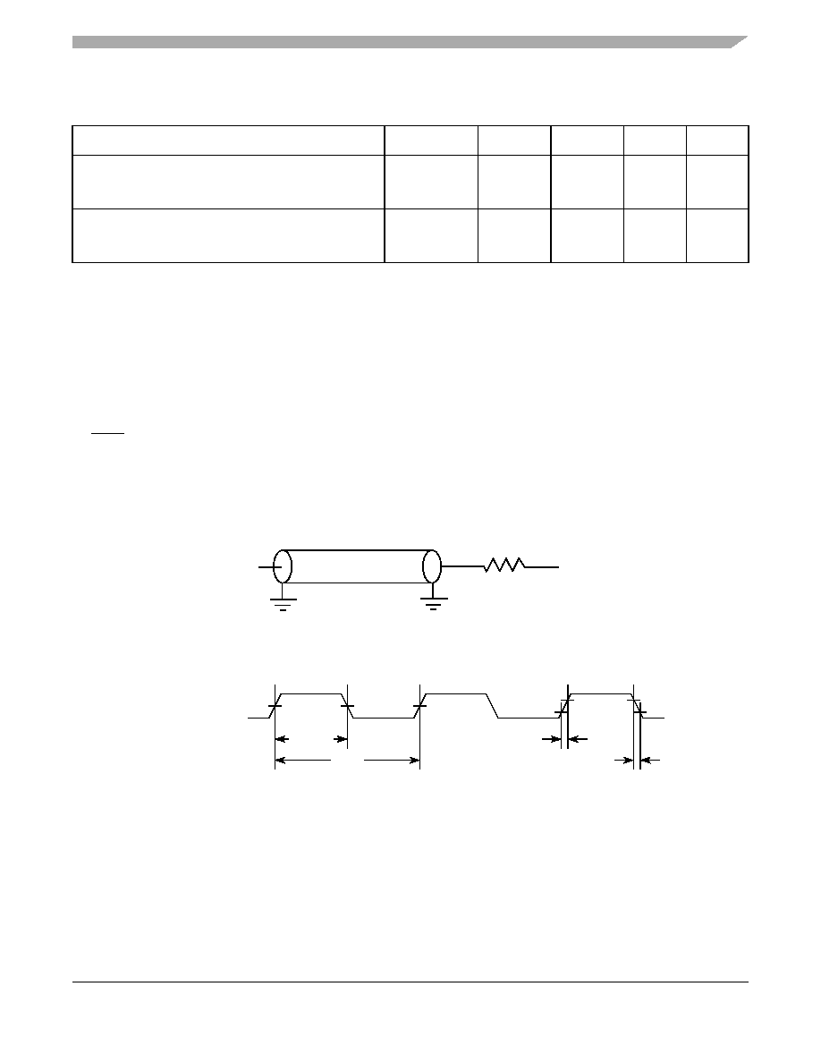
This figure provides the AC test load for TDO and the boundary-scan outputs.
Figure 40. AC Test Load for the JTAG Interface
This figure provides the JTAG clock input timing diagram.
Figure 41. JTAG Clock Input Timing Diagram
Output hold times:
Boundary-scan data
TDO
tJTKLDX
tJTKLOX
2
—
ns
5
JTAG external clock to output high impedance:
Boundary-scan data
TDO
tJTKLDZ
tJTKLOZ
2
19
9
ns
5, 6
Notes:
1. All outputs are measured from the midpoint voltage of the falling/rising edge of tTCLK to the midpoint of the signal in question.
The output timings are measured at the pins. All output timings assume a purely resistive 50-
load (see Figure 40).
Time-of-flight delays must be added for trace lengths, vias, and connectors in the system.
2. The symbols used for timing specifications follow the pattern of t(first two letters of functional block)(signal)(state) (reference)(state) for
inputs and t(first two letters of functional block)(reference)(state)(signal)(state) for outputs. For example, tJTDVKH symbolizes JTAG device
timing (JT) with respect to the time data input signals (D) reaching the valid state (V) relative to the tJTG clock reference (K)
going to the high (H) state or setup time. Also, tJTDXKH symbolizes JTAG timing (JT) with respect to the time data input signals
(D) went invalid (X) relative to the tJTG clock reference (K) going to the high (H) state. Note that, in general, the clock reference
symbol representation is based on three letters representing the clock of a particular functional. For rise and fall times, the
latter convention is used with the appropriate letter: R (rise) or F (fall).
3. TRST is an asynchronous level sensitive signal. The setup time is for test purposes only.
4. Non-JTAG signal input timing with respect to tTCLK.
5. Non-JTAG signal output timing with respect to tTCLK.
6. Guaranteed by design and characterization.
Table 42. JTAG AC Timing Specifications (Independent of SYS_CLK_IN) 1 (continued)
At recommended operating conditions (see Table 2).
Parameter
Symbol2
Min
Max
Unit
Note
Output
Z0 = 50
NVDD/2
RL = 50
JTAG
tJTKHKL
tJTGR
External Clock
VM
tJTG
tJTGF
VM = Midpoint Voltage (NVDD/2)
相关PDF资料 |
PDF描述 |
|---|---|
| EBA22DTMH | CONN EDGECARD 44POS R/A .125 SLD |
| EBA22DTMD | CONN EDGECARD 44POS R/A .125 SLD |
| EBM36DCSN | CONN EDGECARD 72POS DIP .156 SLD |
| EBA22DTBN | CONN EDGECARD 44POS R/A .125 SLD |
| EBM36DCSH | CONN EDGECARD 72POS DIP .156 SLD |
相关代理商/技术参数 |
参数描述 |
|---|---|
| MPC8308-NSG | 功能描述:开发板和工具包 - 其他处理器 MPC8308-NSG RoHS:否 制造商:Freescale Semiconductor 产品:Development Systems 工具用于评估:P3041 核心:e500mc 接口类型:I2C, SPI, USB 工作电源电压: |
| MPC8308-NSG | 制造商:Freescale Semiconductor 功能描述:MPC8308-NSG*NIC* |
| MPC8308-RDB | 功能描述:开发板和工具包 - 其他处理器 Refer. Board MPC8308 RoHS:否 制造商:Freescale Semiconductor 产品:Development Systems 工具用于评估:P3041 核心:e500mc 接口类型:I2C, SPI, USB 工作电源电压: |
| MPC8308-RDB-PROMO | 制造商:Freescale 功能描述:Motherboards MPC8308 PowerQuicc II DDR2 10Mbps/100Mbps/1000Mbps Linux Kernel |
| MPC8308-SOM | 功能描述:开发板和工具包 - 其他处理器 For MPC8308 Ethernet USB 32bit RoHS:否 制造商:Freescale Semiconductor 产品:Development Systems 工具用于评估:P3041 核心:e500mc 接口类型:I2C, SPI, USB 工作电源电压: |
发布紧急采购,3分钟左右您将得到回复。