- 您现在的位置:买卖IC网 > PDF目录4073 > MPC8315ECVRAFDA (Freescale Semiconductor)MPU POWERQUICC II PRO 620-PBGA PDF资料下载
参数资料
| 型号: | MPC8315ECVRAFDA |
| 厂商: | Freescale Semiconductor |
| 文件页数: | 11/106页 |
| 文件大小: | 0K |
| 描述: | MPU POWERQUICC II PRO 620-PBGA |
| 标准包装: | 36 |
| 系列: | MPC83xx |
| 处理器类型: | 32-位 MPC83xx PowerQUICC II Pro |
| 速度: | 333MHz |
| 电压: | 1V |
| 安装类型: | 表面贴装 |
| 封装/外壳: | 620-BBGA 裸露焊盘 |
| 供应商设备封装: | 620-PBGA(29x29) |
| 包装: | 托盘 |
第1页第2页第3页第4页第5页第6页第7页第8页第9页第10页当前第11页第12页第13页第14页第15页第16页第17页第18页第19页第20页第21页第22页第23页第24页第25页第26页第27页第28页第29页第30页第31页第32页第33页第34页第35页第36页第37页第38页第39页第40页第41页第42页第43页第44页第45页第46页第47页第48页第49页第50页第51页第52页第53页第54页第55页第56页第57页第58页第59页第60页第61页第62页第63页第64页第65页第66页第67页第68页第69页第70页第71页第72页第73页第74页第75页第76页第77页第78页第79页第80页第81页第82页第83页第84页第85页第86页第87页第88页第89页第90页第91页第92页第93页第94页第95页第96页第97页第98页第99页第100页第101页第102页第103页第104页第105页第106页
MPC8315E PowerQUICC II Pro Processor Hardware Specifications, Rev. 2
12
Freescale Semiconductor
Electrical Characteristics
3.2
Power Sequencing
The MPC8315E does not require the core supply voltage (VDD and VDDC) and I/O supply voltages
(GVDD, LVDDx_ON, LVDDx_OFF, NVDDx_ON and NVDDx_OFF) to be applied in any particular
order. During the power ramp up, before the power supplies are stable, if the I/O voltages are supplied
before the core voltage, there may be a period of time when all input and output pins be actively driven
and cause contention and/or excessive current. In order to avoid actively driving the I/O pins and to
eliminate excessive current draw, apply the continuous core voltage (VDDC) before the continuous I/O
voltages (LVDDx_ON and NVDDx_ON) and switchable core voltage (VDD) before the switchable I/O
voltages (GVDD, LVDDx_OFF, and NVDDx_OFF). PORESET should be asserted before the continuous
power supplies fully ramp up. In the case where the core voltage is applied first, the core voltage supply
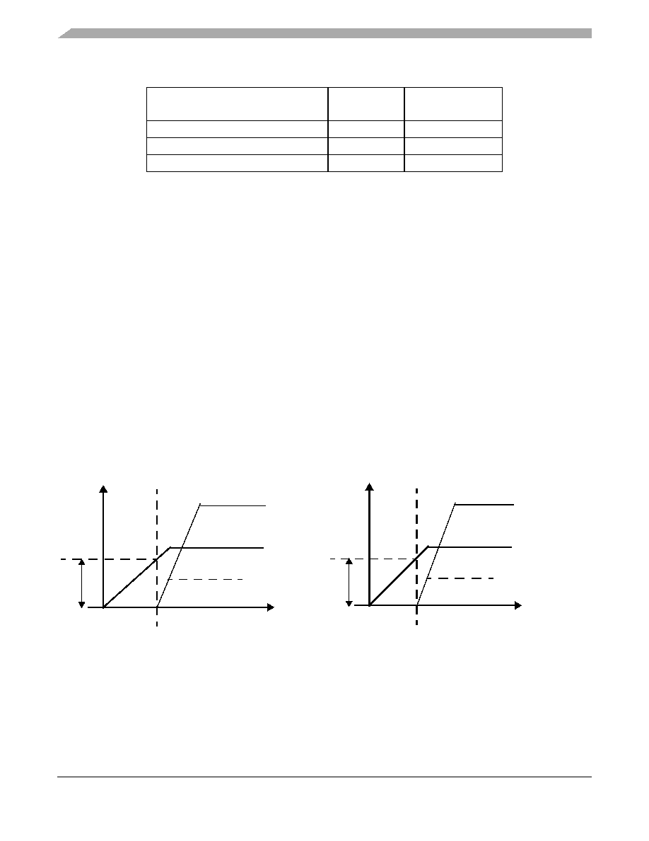
must rise to 90% of its nominal value before the I/O supplies reach 0.7 V, see Figure 3. Once all the power
supplies are stable, wait for a minimum of 32 clock cycles before negating PORESET.
The I/O power supply ramp-up slew rate should be slower than 4V/100 s, this requirement is for ESD
circuit.
This figure shows the power-up sequencing for switchable and continuous supplies.
Figure 3. Power-Up Sequencing
When switching from normal mode to D3 warm (standby) mode, first turn off the switchable I/O voltage
supply and then turn off the switchable core voltage supply. Similarly, when switching from D3 warm
(standby) mode to normal mode, first turn on the switchable core voltage supply and then turn on the
switchable I/O voltage supply.
DUART, system control, I2C, JTAG,SPI
42
NVDD = 3.3 V
GPIO signals
42
NVDD = 3.3 V
eTSEC
42
LVDD = 3.3 V / 2.5 V
1 Output Impedance can also be adjusted through configurable options in DDR
Control Driver Register (DDRCDR). See the MPC8315E PowerQUICC II Pro
Integrated Host Processor Family Reference Manual.
Table 3. Output Drive Capability (continued)
Driver Type
Output
Impedance (
)
Supply
Voltage
Continuous I/O Voltage
Continuous Core Voltage
0.7 V
90%
t
V
Switchable I/O Voltage
Switchable Core Voltage (VDD)
0.7 V
90%
t
V
Power sequence for continuous power supplies
Power sequence for switchable power supplies
相关PDF资料 |
PDF描述 |
|---|---|
| AM1808BZCE4 | IC ARM9 MPU 361NFBGA |
| AM1808BZWTD4 | IC ARM9 CORTEX MCU 361NFBGA |
| AM1808BZCE3 | IC ARM9 CORTEX MCU 361NFBGA |
| AMC60DRTN-S93 | CONN EDGECARD 120PS DIP .100 SLD |
| AMC60DRTH-S93 | CONN EDGECARD 120PS DIP .100 SLD |
相关代理商/技术参数 |
参数描述 |
|---|---|
| MPC8315ECVRAGDA | 功能描述:微处理器 - MPU ENCRYPT RoHS:否 制造商:Atmel 处理器系列:SAMA5D31 核心:ARM Cortex A5 数据总线宽度:32 bit 最大时钟频率:536 MHz 程序存储器大小:32 KB 数据 RAM 大小:128 KB 接口类型:CAN, Ethernet, LIN, SPI,TWI, UART, USB 工作电源电压:1.8 V to 3.3 V 最大工作温度:+ 85 C 安装风格:SMD/SMT 封装 / 箱体:FBGA-324 |
| MPC8315E-RDB | 功能描述:处理器 - 专门应用 PROCESSOR BD RoHS:否 制造商:Freescale Semiconductor 类型:Multimedia Applications 核心:ARM Cortex A9 处理器系列:i.MX6 数据总线宽度:32 bit 最大时钟频率:1 GHz 指令/数据缓存: 数据 RAM 大小:128 KB 数据 ROM 大小: 工作电源电压: 最大工作温度:+ 95 C 安装风格:SMD/SMT 封装 / 箱体:MAPBGA-432 |
| MPC8315E-RDBA | 功能描述:开发板和工具包 - 其他处理器 PROCESSOR BD RoHS:否 制造商:Freescale Semiconductor 产品:Development Systems 工具用于评估:P3041 核心:e500mc 接口类型:I2C, SPI, USB 工作电源电压: |
| MPC8315E-RDBA | 制造商:Freescale Semiconductor 功能描述:MPC8315E-RDB Reference Platform |
| MPC8315EVRADDA | 功能描述:微处理器 - MPU ENCRYPT RoHS:否 制造商:Atmel 处理器系列:SAMA5D31 核心:ARM Cortex A5 数据总线宽度:32 bit 最大时钟频率:536 MHz 程序存储器大小:32 KB 数据 RAM 大小:128 KB 接口类型:CAN, Ethernet, LIN, SPI,TWI, UART, USB 工作电源电压:1.8 V to 3.3 V 最大工作温度:+ 85 C 安装风格:SMD/SMT 封装 / 箱体:FBGA-324 |
发布紧急采购,3分钟左右您将得到回复。