- 您现在的位置:买卖IC网 > PDF目录4073 > MPC8315ECVRAFDA (Freescale Semiconductor)MPU POWERQUICC II PRO 620-PBGA PDF资料下载
参数资料
| 型号: | MPC8315ECVRAFDA |
| 厂商: | Freescale Semiconductor |
| 文件页数: | 35/106页 |
| 文件大小: | 0K |
| 描述: | MPU POWERQUICC II PRO 620-PBGA |
| 标准包装: | 36 |
| 系列: | MPC83xx |
| 处理器类型: | 32-位 MPC83xx PowerQUICC II Pro |
| 速度: | 333MHz |
| 电压: | 1V |
| 安装类型: | 表面贴装 |
| 封装/外壳: | 620-BBGA 裸露焊盘 |
| 供应商设备封装: | 620-PBGA(29x29) |
| 包装: | 托盘 |
第1页第2页第3页第4页第5页第6页第7页第8页第9页第10页第11页第12页第13页第14页第15页第16页第17页第18页第19页第20页第21页第22页第23页第24页第25页第26页第27页第28页第29页第30页第31页第32页第33页第34页当前第35页第36页第37页第38页第39页第40页第41页第42页第43页第44页第45页第46页第47页第48页第49页第50页第51页第52页第53页第54页第55页第56页第57页第58页第59页第60页第61页第62页第63页第64页第65页第66页第67页第68页第69页第70页第71页第72页第73页第74页第75页第76页第77页第78页第79页第80页第81页第82页第83页第84页第85页第86页第87页第88页第89页第90页第91页第92页第93页第94页第95页第96页第97页第98页第99页第100页第101页第102页第103页第104页第105页第106页
MPC8315E PowerQUICC II Pro Processor Hardware Specifications, Rev. 2
34
Freescale Semiconductor
Ethernet: Three-Speed Ethernet, MII Management
9.5
SGMII Interface Electrical Characteristics
Each SGMII port features a 4-wire AC-Coupled serial link from the dedicated SerDes interface of
output pin of the SerDes transmitter differential pair features 50-
output impedance. Each input of the
SerDes receiver differential pair features 50-
on-die termination to XCOREVSS. The reference circuit
of the SerDes transmitter and receiver is shown in Figure 49.
When an eTSEC port is configured to operate in SGMII mode, the parallel interface’s output signals of
this eTSEC port can be left floating. The input signals should be terminated based on the guidelines
described in Section 26.4, “Connection Recommendations,” as long as such termination does not violate
the desired POR configuration requirement on these pins, if applicable.
When operating in SGMII mode, the TSEC_GTX_CLK125 clock is not required for this port. Instead,
SerDes reference clock is required on SD_REF_CLK and SD_REF_CLK pins.
9.5.1
DC Requirements for SGMII SD_REF_CLK and SD_REF_CLK
The characteristics and DC requirements of the separate SerDes reference clock are described in
9.5.2
AC Requirements for SGMII SD_REF_CLK and SD_REF_CLK
This table lists the SGMII SerDes reference clock AC requirements. Please note that SD_REF_CLK and
SD_REF_CLK are not intended to be used with, and should not be clocked by, a spread spectrum clock
source.
9.5.3
SGMII Transmitter and Receiver DC Electrical Characteristics
characteristics. Transmitter DC characteristics are measured at the transmitter outputs (SD_TX[n] and
SD_TX[n]) as depicted in Figure 17.
Note:
1. The timer can operate on rtc_clock or tmr_clock. These clocks get muxed and any one of them can be selected.
2. Asynchronous signals.
3. Inputs need to be stable at least one TMR clock.
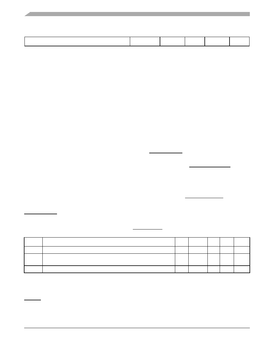
Table 34. SD_REF_CLK and SD_REF_CLK AC Requirements
Symbol
Parameter Description
Min
Typical
Max
Unit
Note
tREF
REFCLK cycle time
—
8
—
ns
—
tREFCJ
REFCLK cycle-to-cycle jitter. Difference in the period of any two adjacent
REFCLK cycles
——
100
ps
—
tREFPJ
Phase jitter. Deviation in edge location with respect to mean edge location
–50
—
50
ps
—
Table 33. 1588 Timer AC Specifications (continued)
Parameter
Symbol
Min
Max
Unit
Note
相关PDF资料 |
PDF描述 |
|---|---|
| AM1808BZCE4 | IC ARM9 MPU 361NFBGA |
| AM1808BZWTD4 | IC ARM9 CORTEX MCU 361NFBGA |
| AM1808BZCE3 | IC ARM9 CORTEX MCU 361NFBGA |
| AMC60DRTN-S93 | CONN EDGECARD 120PS DIP .100 SLD |
| AMC60DRTH-S93 | CONN EDGECARD 120PS DIP .100 SLD |
相关代理商/技术参数 |
参数描述 |
|---|---|
| MPC8315ECVRAGDA | 功能描述:微处理器 - MPU ENCRYPT RoHS:否 制造商:Atmel 处理器系列:SAMA5D31 核心:ARM Cortex A5 数据总线宽度:32 bit 最大时钟频率:536 MHz 程序存储器大小:32 KB 数据 RAM 大小:128 KB 接口类型:CAN, Ethernet, LIN, SPI,TWI, UART, USB 工作电源电压:1.8 V to 3.3 V 最大工作温度:+ 85 C 安装风格:SMD/SMT 封装 / 箱体:FBGA-324 |
| MPC8315E-RDB | 功能描述:处理器 - 专门应用 PROCESSOR BD RoHS:否 制造商:Freescale Semiconductor 类型:Multimedia Applications 核心:ARM Cortex A9 处理器系列:i.MX6 数据总线宽度:32 bit 最大时钟频率:1 GHz 指令/数据缓存: 数据 RAM 大小:128 KB 数据 ROM 大小: 工作电源电压: 最大工作温度:+ 95 C 安装风格:SMD/SMT 封装 / 箱体:MAPBGA-432 |
| MPC8315E-RDBA | 功能描述:开发板和工具包 - 其他处理器 PROCESSOR BD RoHS:否 制造商:Freescale Semiconductor 产品:Development Systems 工具用于评估:P3041 核心:e500mc 接口类型:I2C, SPI, USB 工作电源电压: |
| MPC8315E-RDBA | 制造商:Freescale Semiconductor 功能描述:MPC8315E-RDB Reference Platform |
| MPC8315EVRADDA | 功能描述:微处理器 - MPU ENCRYPT RoHS:否 制造商:Atmel 处理器系列:SAMA5D31 核心:ARM Cortex A5 数据总线宽度:32 bit 最大时钟频率:536 MHz 程序存储器大小:32 KB 数据 RAM 大小:128 KB 接口类型:CAN, Ethernet, LIN, SPI,TWI, UART, USB 工作电源电压:1.8 V to 3.3 V 最大工作温度:+ 85 C 安装风格:SMD/SMT 封装 / 箱体:FBGA-324 |
发布紧急采购,3分钟左右您将得到回复。