- 您现在的位置:买卖IC网 > PDF目录4073 > MPC8315ECVRAFDA (Freescale Semiconductor)MPU POWERQUICC II PRO 620-PBGA PDF资料下载
参数资料
| 型号: | MPC8315ECVRAFDA |
| 厂商: | Freescale Semiconductor |
| 文件页数: | 71/106页 |
| 文件大小: | 0K |
| 描述: | MPU POWERQUICC II PRO 620-PBGA |
| 标准包装: | 36 |
| 系列: | MPC83xx |
| 处理器类型: | 32-位 MPC83xx PowerQUICC II Pro |
| 速度: | 333MHz |
| 电压: | 1V |
| 安装类型: | 表面贴装 |
| 封装/外壳: | 620-BBGA 裸露焊盘 |
| 供应商设备封装: | 620-PBGA(29x29) |
| 包装: | 托盘 |
第1页第2页第3页第4页第5页第6页第7页第8页第9页第10页第11页第12页第13页第14页第15页第16页第17页第18页第19页第20页第21页第22页第23页第24页第25页第26页第27页第28页第29页第30页第31页第32页第33页第34页第35页第36页第37页第38页第39页第40页第41页第42页第43页第44页第45页第46页第47页第48页第49页第50页第51页第52页第53页第54页第55页第56页第57页第58页第59页第60页第61页第62页第63页第64页第65页第66页第67页第68页第69页第70页当前第71页第72页第73页第74页第75页第76页第77页第78页第79页第80页第81页第82页第83页第84页第85页第86页第87页第88页第89页第90页第91页第92页第93页第94页第95页第96页第97页第98页第99页第100页第101页第102页第103页第104页第105页第106页
MPC8315E PowerQUICC II Pro Processor Hardware Specifications, Rev. 2
Freescale Semiconductor
67
PCI Express
16.5
Receiver Compliance Eye Diagrams
The RX eye diagram in Figure 51 is specified using the passive compliance/test measurement load (see
Figure 52) in place of any real PCI Express RX component. In general, the minimum receiver eye diagram
measured with the compliance/test measurement load (see Figure 52) is larger than the minimum receiver
eye diagram measured over a range of systems at the input receiver of any real PCI Express component.
The degraded eye diagram at the input Receiver is due to traces internal to the package as well as silicon
parasitic characteristics which cause the real PCI Express component to vary in impedance from the
compliance/test measurement load. The input receiver eye diagram is implementation specific and is not
specified. RX component designer should provide additional margin to adequately compensate for the
degraded minimum Receiver eye diagram (shown in Figure 51) expected at the input receiver based on an
adequate combination of system simulations and the return loss measured looking into the RX package
and silicon. The RX eye diagram must be aligned in time using the jitter median to locate the center of the
eye diagram.
The eye diagram must be valid for any 250 consecutive UIs.
A recovered TX UI is calculated over 3500 consecutive unit intervals of sample data. The eye diagram is
created using all edges of the 250 consecutive UI in the center of the 3500 UI used for calculating the TX
UI.
NOTE
The reference impedance for return loss measurements is 50
to ground for
both the D+ and D- line (that is, as measured by a Vector Network Analyzer
with 50
probes—see Figure 52). Note that the series capacitors,
CPEACCTX, are optional for the return loss measurement.
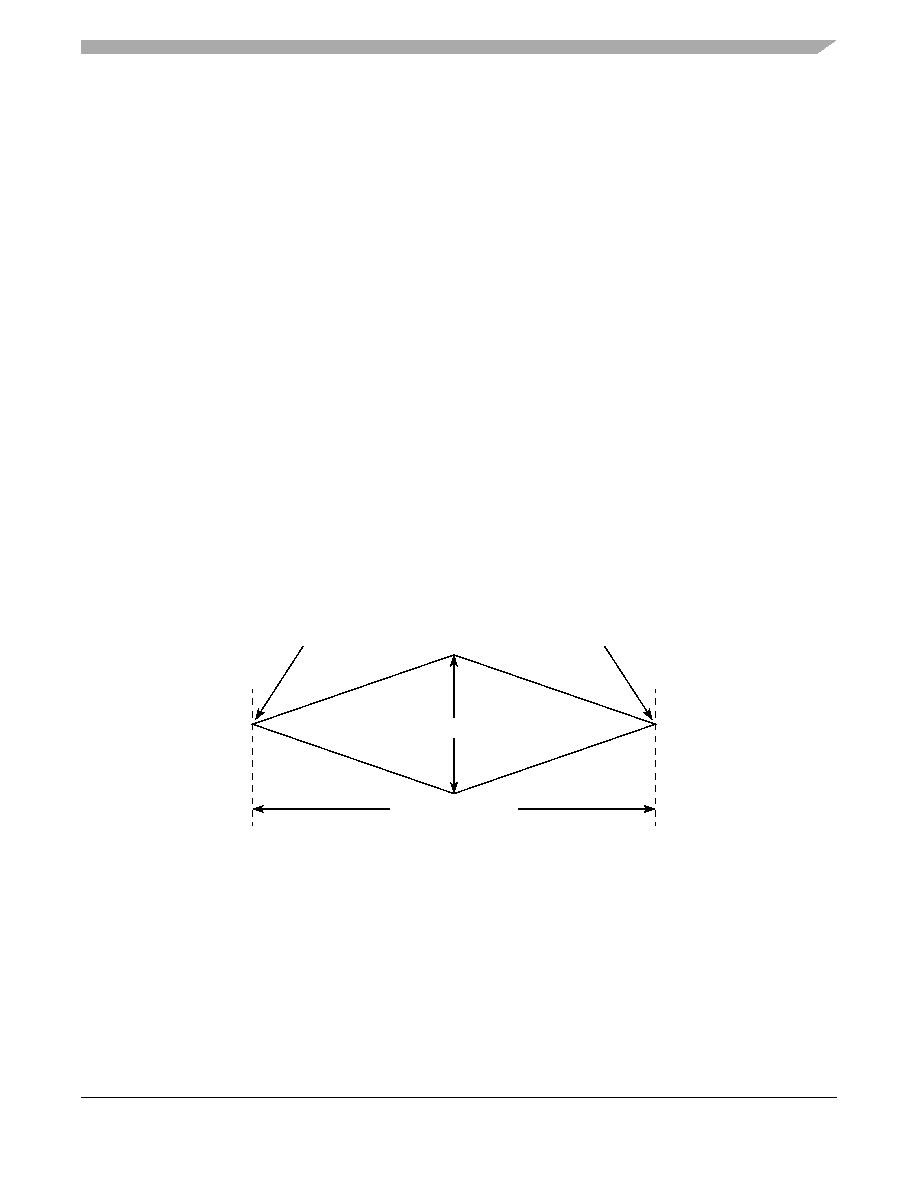
Figure 51. Minimum Receiver Eye Timing and Voltage Compliance Specification
16.5.1
Compliance Test and Measurement Load
The AC timing and voltage parameters must be verified at the measurement point, as specified within
0.2 inches of the package pins, into a test/measurement load shown in Figure 52.
VRX-DIFFp-p-MIN > 175 mV
0.4 UI = TRX-EYE-MIN
VRX-DIFF = 0 mV
(D+ D– Crossing Point)
VRX-DIFF = 0 mV
(D+ D– Crossing Point)
相关PDF资料 |
PDF描述 |
|---|---|
| AM1808BZCE4 | IC ARM9 MPU 361NFBGA |
| AM1808BZWTD4 | IC ARM9 CORTEX MCU 361NFBGA |
| AM1808BZCE3 | IC ARM9 CORTEX MCU 361NFBGA |
| AMC60DRTN-S93 | CONN EDGECARD 120PS DIP .100 SLD |
| AMC60DRTH-S93 | CONN EDGECARD 120PS DIP .100 SLD |
相关代理商/技术参数 |
参数描述 |
|---|---|
| MPC8315ECVRAGDA | 功能描述:微处理器 - MPU ENCRYPT RoHS:否 制造商:Atmel 处理器系列:SAMA5D31 核心:ARM Cortex A5 数据总线宽度:32 bit 最大时钟频率:536 MHz 程序存储器大小:32 KB 数据 RAM 大小:128 KB 接口类型:CAN, Ethernet, LIN, SPI,TWI, UART, USB 工作电源电压:1.8 V to 3.3 V 最大工作温度:+ 85 C 安装风格:SMD/SMT 封装 / 箱体:FBGA-324 |
| MPC8315E-RDB | 功能描述:处理器 - 专门应用 PROCESSOR BD RoHS:否 制造商:Freescale Semiconductor 类型:Multimedia Applications 核心:ARM Cortex A9 处理器系列:i.MX6 数据总线宽度:32 bit 最大时钟频率:1 GHz 指令/数据缓存: 数据 RAM 大小:128 KB 数据 ROM 大小: 工作电源电压: 最大工作温度:+ 95 C 安装风格:SMD/SMT 封装 / 箱体:MAPBGA-432 |
| MPC8315E-RDBA | 功能描述:开发板和工具包 - 其他处理器 PROCESSOR BD RoHS:否 制造商:Freescale Semiconductor 产品:Development Systems 工具用于评估:P3041 核心:e500mc 接口类型:I2C, SPI, USB 工作电源电压: |
| MPC8315E-RDBA | 制造商:Freescale Semiconductor 功能描述:MPC8315E-RDB Reference Platform |
| MPC8315EVRADDA | 功能描述:微处理器 - MPU ENCRYPT RoHS:否 制造商:Atmel 处理器系列:SAMA5D31 核心:ARM Cortex A5 数据总线宽度:32 bit 最大时钟频率:536 MHz 程序存储器大小:32 KB 数据 RAM 大小:128 KB 接口类型:CAN, Ethernet, LIN, SPI,TWI, UART, USB 工作电源电压:1.8 V to 3.3 V 最大工作温度:+ 85 C 安装风格:SMD/SMT 封装 / 箱体:FBGA-324 |
发布紧急采购,3分钟左右您将得到回复。