- 您现在的位置:买卖IC网 > PDF目录4056 > MPC8377VRALG (Freescale Semiconductor)MPU POWERQUICC II PRO 689-PBGA PDF资料下载
参数资料
| 型号: | MPC8377VRALG |
| 厂商: | Freescale Semiconductor |
| 文件页数: | 10/127页 |
| 文件大小: | 0K |
| 描述: | MPU POWERQUICC II PRO 689-PBGA |
| 标准包装: | 27 |
| 系列: | MPC83xx |
| 处理器类型: | 32-位 MPC83xx PowerQUICC II Pro |
| 速度: | 667MHz |
| 电压: | 1V |
| 安装类型: | 表面贴装 |
| 封装/外壳: | 689-BBGA 裸露焊盘 |
| 供应商设备封装: | 689-TEPBGA II(31x31) |
| 包装: | 托盘 |
第1页第2页第3页第4页第5页第6页第7页第8页第9页当前第10页第11页第12页第13页第14页第15页第16页第17页第18页第19页第20页第21页第22页第23页第24页第25页第26页第27页第28页第29页第30页第31页第32页第33页第34页第35页第36页第37页第38页第39页第40页第41页第42页第43页第44页第45页第46页第47页第48页第49页第50页第51页第52页第53页第54页第55页第56页第57页第58页第59页第60页第61页第62页第63页第64页第65页第66页第67页第68页第69页第70页第71页第72页第73页第74页第75页第76页第77页第78页第79页第80页第81页第82页第83页第84页第85页第86页第87页第88页第89页第90页第91页第92页第93页第94页第95页第96页第97页第98页第99页第100页第101页第102页第103页第104页第105页第106页第107页第108页第109页第110页第111页第112页第113页第114页第115页第116页第117页第118页第119页第120页第121页第122页第123页第124页第125页第126页第127页
MPC8377E PowerQUICC II Pro Processor Hardware Specifications, Rev. 8
Freescale Semiconductor
107
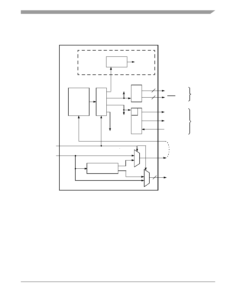
23 Clocking
This figure shows the internal distribution of clocks within this chip.
Figure 64. Clock Subsystem
The primary clock source for the device can be one of two inputs, CLKIN or PCI_CLK, depending on
whether the device is configured in PCI host or PCI agent mode. When the device is configured as a PCI
host device, CLKIN is its primary input clock. CLKIN feeds the PCI clock divider (
÷2) and the
multiplexors for PCI_SYNC_OUT and PCI_CLK_OUT. The CFG_CLKIN_DIV configuration input
selects whether CLKIN or CLKIN/2 is driven out on the PCI_SYNC_OUT signal. The OCCR[PCICOEn]
parameters select whether CFG_CLKIN_DIV is driven out on the PCI_CLK_OUTn signals.
PCI_SYNC_OUT is connected externally to PCI_SYNC_IN to allow the internal clock subsystem to
synchronize to the system PCI clocks. PCI_SYNC_OUT must be connected properly to PCI_SYNC_IN,
with equal delay to all PCI agent devices in the system, to allow the device to function. When the device
is configured as a PCI agent device, PCI_CLK is the primary input clock. When the device is configured
as a PCI agent device the CLKIN signal should be tied to GND.
Core PLL
System PLL
DDR
LBIU
LSYNC_IN
LSYNC_OUT
LCLK[0:2]
MCK[0:5]
core_clk
e300 core
csb_clk to rest
CLKIN
csb_clk
6
DDR
Memory
Local Bus
PCI_CLK[0:4]
PCI_SYNC_OUT
PCI_CLK/
Clock
Unit
of the device
ddr_clk
lbiu_clk
CFG_CLKIN_DIV
PCI Clock
PCI_SYNC_IN
Device
Memory
Device
/n
to local bus
memory
controller
to DDR
memory
controller
DLL
Clock
Div
/2
Divider
5
相关PDF资料 |
PDF描述 |
|---|---|
| MPC866PCZP100A | IC MPU POWERQUICC 100MHZ 357PBGA |
| MPC603RRX200LC | IC MPU POWERPC 200MHZ 255-CBGA |
| MC68360ZQ25L | IC MPU QUICC 25MHZ 357-PBGA |
| MC68360VR25L | IC MPU QUICC 25MHZ 357-PBGA |
| MPC8248VRTIEA | IC MPU POWERQUICC II 516-PBGA |
相关代理商/技术参数 |
参数描述 |
|---|---|
| MPC8377VRALGA | 功能描述:微处理器 - MPU 8377 PBGA ST PbFr No ENC RoHS:否 制造商:Atmel 处理器系列:SAMA5D31 核心:ARM Cortex A5 数据总线宽度:32 bit 最大时钟频率:536 MHz 程序存储器大小:32 KB 数据 RAM 大小:128 KB 接口类型:CAN, Ethernet, LIN, SPI,TWI, UART, USB 工作电源电压:1.8 V to 3.3 V 最大工作温度:+ 85 C 安装风格:SMD/SMT 封装 / 箱体:FBGA-324 |
| MPC8377VRANDA | 制造商:FREESCALE 制造商全称:Freescale Semiconductor, Inc 功能描述:PowerQUICC? II Pro Processor Hardware Specifications |
| MPC8377VRANFA | 制造商:FREESCALE 制造商全称:Freescale Semiconductor, Inc 功能描述:PowerQUICC? II Pro Processor Hardware Specifications |
| MPC8377VRANG | 功能描述:微处理器 - MPU 837X Non-Encrypted RoHS:否 制造商:Atmel 处理器系列:SAMA5D31 核心:ARM Cortex A5 数据总线宽度:32 bit 最大时钟频率:536 MHz 程序存储器大小:32 KB 数据 RAM 大小:128 KB 接口类型:CAN, Ethernet, LIN, SPI,TWI, UART, USB 工作电源电压:1.8 V to 3.3 V 最大工作温度:+ 85 C 安装风格:SMD/SMT 封装 / 箱体:FBGA-324 |
| MPC8377VRANGA | 功能描述:微处理器 - MPU 8377 PBGA ST PbFr No ENC RoHS:否 制造商:Atmel 处理器系列:SAMA5D31 核心:ARM Cortex A5 数据总线宽度:32 bit 最大时钟频率:536 MHz 程序存储器大小:32 KB 数据 RAM 大小:128 KB 接口类型:CAN, Ethernet, LIN, SPI,TWI, UART, USB 工作电源电压:1.8 V to 3.3 V 最大工作温度:+ 85 C 安装风格:SMD/SMT 封装 / 箱体:FBGA-324 |
发布紧急采购,3分钟左右您将得到回复。