- 您现在的位置:买卖IC网 > PDF目录4056 > MPC8377VRALG (Freescale Semiconductor)MPU POWERQUICC II PRO 689-PBGA PDF资料下载
参数资料
| 型号: | MPC8377VRALG |
| 厂商: | Freescale Semiconductor |
| 文件页数: | 107/127页 |
| 文件大小: | 0K |
| 描述: | MPU POWERQUICC II PRO 689-PBGA |
| 标准包装: | 27 |
| 系列: | MPC83xx |
| 处理器类型: | 32-位 MPC83xx PowerQUICC II Pro |
| 速度: | 667MHz |
| 电压: | 1V |
| 安装类型: | 表面贴装 |
| 封装/外壳: | 689-BBGA 裸露焊盘 |
| 供应商设备封装: | 689-TEPBGA II(31x31) |
| 包装: | 托盘 |
第1页第2页第3页第4页第5页第6页第7页第8页第9页第10页第11页第12页第13页第14页第15页第16页第17页第18页第19页第20页第21页第22页第23页第24页第25页第26页第27页第28页第29页第30页第31页第32页第33页第34页第35页第36页第37页第38页第39页第40页第41页第42页第43页第44页第45页第46页第47页第48页第49页第50页第51页第52页第53页第54页第55页第56页第57页第58页第59页第60页第61页第62页第63页第64页第65页第66页第67页第68页第69页第70页第71页第72页第73页第74页第75页第76页第77页第78页第79页第80页第81页第82页第83页第84页第85页第86页第87页第88页第89页第90页第91页第92页第93页第94页第95页第96页第97页第98页第99页第100页第101页第102页第103页第104页第105页第106页当前第107页第108页第109页第110页第111页第112页第113页第114页第115页第116页第117页第118页第119页第120页第121页第122页第123页第124页第125页第126页第127页
MPC8377E PowerQUICC II Pro Processor Hardware Specifications, Rev. 8
80
Freescale Semiconductor
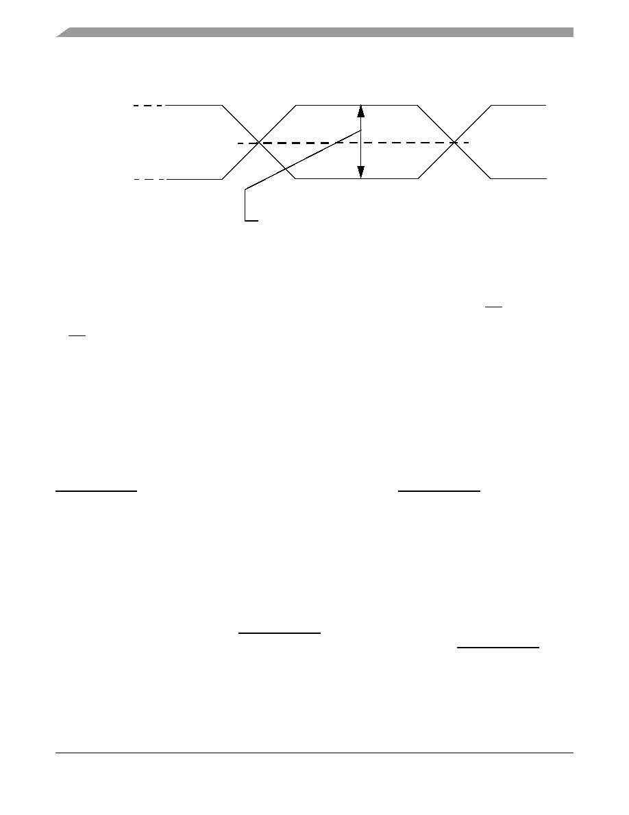
Figure 51. Differential Voltage Definitions for Transmitter or Receiver
To illustrate these definitions using real values, consider the case of a CML (Current Mode Logic)
transmitter that has a common mode voltage of 2.25 V and each of its outputs, TD and TD, has a swing
that goes between 2.5 V and 2.0 V. Using these values, the peak-to-peak voltage swing of each signal (TD
or TD) is 500 mVp-p, which is referred as the single-ended swing for each signal. In this example, since
the differential signaling environment is fully symmetrical, the transmitter output’s differential swing
(VOD) has the same amplitude as each signal’s single-ended swing. The differential output signal ranges
between 500 mV and –500 mV, in other words, VOD is 500 mV in one phase and –500 mV in the other
phase. The peak differential voltage (VDIFFp) is 500 mV. The peak-to-peak differential voltage (VDIFFp-p)
is 1000 mVp-p.
21.2
SerDes Reference Clocks
The SerDes reference clock inputs are applied to an internal PLL whose output creates the clock used by
the corresponding SerDes lanes. The SerDes reference clocks inputs are SD1_REF_CLK and
SD1_REF_CLK for both lanes of SerDes1, and SD2_REF_CLK and SD2_REF_CLK for both lanes of
SerDes2.
The following sections describe the SerDes reference clock requirements and some application
information.
21.2.1
SerDes Reference Clock Receiver Characteristics
Figure 52 shows a receiver reference diagram of the SerDes reference clocks.
SerDes Reference Clock Receiver Reference Circuit Structure
—The SDn_REF_CLK and SDn_REF_CLK are internally AC-coupled differential inputs as
shown in Figure 52. Each differential clock input (SDn_REF_CLK or SDn_REF_CLK) has a
50
Ω termination to SGND_SRDSn (xcorevss) followed by on-chip AC-coupling.
— The external reference clock driver must be able to drive this termination.
Differential Swing, VID or VOD = A – B
A Volts
B Volts
SD
n_TX or
SD
n_RX
SD
n_TX or
SD
n_RX
Differential Peak Voltage, VDIFFp = |A – B|
Differential Peak-Peak Voltage, VDIFFpp = 2
× VDIFFp (not shown)
Vcm = (A + B)/2
相关PDF资料 |
PDF描述 |
|---|---|
| MPC866PCZP100A | IC MPU POWERQUICC 100MHZ 357PBGA |
| MPC603RRX200LC | IC MPU POWERPC 200MHZ 255-CBGA |
| MC68360ZQ25L | IC MPU QUICC 25MHZ 357-PBGA |
| MC68360VR25L | IC MPU QUICC 25MHZ 357-PBGA |
| MPC8248VRTIEA | IC MPU POWERQUICC II 516-PBGA |
相关代理商/技术参数 |
参数描述 |
|---|---|
| MPC8377VRALGA | 功能描述:微处理器 - MPU 8377 PBGA ST PbFr No ENC RoHS:否 制造商:Atmel 处理器系列:SAMA5D31 核心:ARM Cortex A5 数据总线宽度:32 bit 最大时钟频率:536 MHz 程序存储器大小:32 KB 数据 RAM 大小:128 KB 接口类型:CAN, Ethernet, LIN, SPI,TWI, UART, USB 工作电源电压:1.8 V to 3.3 V 最大工作温度:+ 85 C 安装风格:SMD/SMT 封装 / 箱体:FBGA-324 |
| MPC8377VRANDA | 制造商:FREESCALE 制造商全称:Freescale Semiconductor, Inc 功能描述:PowerQUICC? II Pro Processor Hardware Specifications |
| MPC8377VRANFA | 制造商:FREESCALE 制造商全称:Freescale Semiconductor, Inc 功能描述:PowerQUICC? II Pro Processor Hardware Specifications |
| MPC8377VRANG | 功能描述:微处理器 - MPU 837X Non-Encrypted RoHS:否 制造商:Atmel 处理器系列:SAMA5D31 核心:ARM Cortex A5 数据总线宽度:32 bit 最大时钟频率:536 MHz 程序存储器大小:32 KB 数据 RAM 大小:128 KB 接口类型:CAN, Ethernet, LIN, SPI,TWI, UART, USB 工作电源电压:1.8 V to 3.3 V 最大工作温度:+ 85 C 安装风格:SMD/SMT 封装 / 箱体:FBGA-324 |
| MPC8377VRANGA | 功能描述:微处理器 - MPU 8377 PBGA ST PbFr No ENC RoHS:否 制造商:Atmel 处理器系列:SAMA5D31 核心:ARM Cortex A5 数据总线宽度:32 bit 最大时钟频率:536 MHz 程序存储器大小:32 KB 数据 RAM 大小:128 KB 接口类型:CAN, Ethernet, LIN, SPI,TWI, UART, USB 工作电源电压:1.8 V to 3.3 V 最大工作温度:+ 85 C 安装风格:SMD/SMT 封装 / 箱体:FBGA-324 |
发布紧急采购,3分钟左右您将得到回复。