- 您现在的位置:买卖IC网 > PDF目录4056 > MPC8377VRALG (Freescale Semiconductor)MPU POWERQUICC II PRO 689-PBGA PDF资料下载
参数资料
| 型号: | MPC8377VRALG |
| 厂商: | Freescale Semiconductor |
| 文件页数: | 36/127页 |
| 文件大小: | 0K |
| 描述: | MPU POWERQUICC II PRO 689-PBGA |
| 标准包装: | 27 |
| 系列: | MPC83xx |
| 处理器类型: | 32-位 MPC83xx PowerQUICC II Pro |
| 速度: | 667MHz |
| 电压: | 1V |
| 安装类型: | 表面贴装 |
| 封装/外壳: | 689-BBGA 裸露焊盘 |
| 供应商设备封装: | 689-TEPBGA II(31x31) |
| 包装: | 托盘 |
第1页第2页第3页第4页第5页第6页第7页第8页第9页第10页第11页第12页第13页第14页第15页第16页第17页第18页第19页第20页第21页第22页第23页第24页第25页第26页第27页第28页第29页第30页第31页第32页第33页第34页第35页当前第36页第37页第38页第39页第40页第41页第42页第43页第44页第45页第46页第47页第48页第49页第50页第51页第52页第53页第54页第55页第56页第57页第58页第59页第60页第61页第62页第63页第64页第65页第66页第67页第68页第69页第70页第71页第72页第73页第74页第75页第76页第77页第78页第79页第80页第81页第82页第83页第84页第85页第86页第87页第88页第89页第90页第91页第92页第93页第94页第95页第96页第97页第98页第99页第100页第101页第102页第103页第104页第105页第106页第107页第108页第109页第110页第111页第112页第113页第114页第115页第116页第117页第118页第119页第120页第121页第122页第123页第124页第125页第126页第127页
MPC8377E PowerQUICC II Pro Processor Hardware Specifications, Rev. 8
16
Freescale Semiconductor
5.2
RESET AC Electrical Characteristics
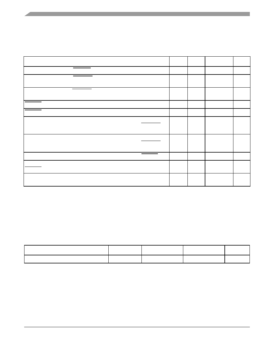
This table provides the reset initialization AC timing specifications of the device.
Table 12 provides the PLL lock times.
6
DDR1 and DDR2 SDRAM
This section describes the DC and AC electrical specifications for the DDR SDRAM interface of the chip.
Note that DDR1 SDRAM is GVDD(typ) = 2.5 V and DDR2 SDRAM is GVDD(typ) = 1.8 V.
Table 11. RESET Initialization Timing Specifications
Parameter/Condition
Min
Max
Unit
Note
Required assertion time of HRESET to activate reset flow
32
—
tPCI_SYNC_IN
Required assertion time of PORESET with stable clock applied to CLKIN when
the device is in PCI host mode
32
—
tCLKIN
Required assertion time of PORESET with stable clock applied to PCI_CLK when
the device is in PCI agent mode
32
—
tPCI_SYNC_IN
HRESET assertion (output)
512
—
tPCI_SYNC_IN
HRESET negation to negation (output)
16
—
tPCI_SYNC_IN
Input setup time for POR config signals (CFG_RESET_SOURCE[0:3],
CFG_CLKIN_DIV, and CFG_LBMUX) with respect to negation of PORESET
when the device is in PCI host mode
4—
tCLKIN
Input setup time for POR config signals (CFG_RESET_SOURCE[0:3],
CFG_CLKIN_DIV, and CFG_LBMUX) with respect to negation of PORESET
when the device is in PCI agent mode
4—
tPCI_SYNC_IN
Input hold time for POR config signals with respect to negation of HRESET
0—
ns
—
Time for the device to turn off POR config signals with respect to the assertion of
HRESET
—4
ns
Time for the device to start driving functional output signals multiplexed with the
POR configuration signals with respect to the negation of HRESET
1—
tPCI_SYNC_IN
Notes:
1. tPCI_SYNC_IN is the clock period of the input clock applied to PCI_SYNC_IN. When the device is In PCI host mode the primary
clock is applied to the CLKIN input, and PCI_SYNC_IN period depends on the value of CFG_CLKIN_DIV. See the
MPC8379E Integrated Host Processor Reference Manual for more details.
2. tCLKIN is the clock period of the input clock applied to CLKIN. It is only valid when the device is in PCI host mode. See the
MPC8379E Integrated Host Processor Reference Manual for more details.
3. POR config signals consists of CFG_RESET_SOURCE[0:3], CFG_LBMUX, and CFG_CLKIN_DIV.
Table 12. PLL Lock Times
Parameter
Min
Max
Unit
Note
PLL lock times
—
100
μs—
Note:
The device guarantees the PLL lock if the clock settings are within spec range. The core clock also depends on the core PLL
ratio. See Section 23, “Clocking,” for more information.
相关PDF资料 |
PDF描述 |
|---|---|
| MPC866PCZP100A | IC MPU POWERQUICC 100MHZ 357PBGA |
| MPC603RRX200LC | IC MPU POWERPC 200MHZ 255-CBGA |
| MC68360ZQ25L | IC MPU QUICC 25MHZ 357-PBGA |
| MC68360VR25L | IC MPU QUICC 25MHZ 357-PBGA |
| MPC8248VRTIEA | IC MPU POWERQUICC II 516-PBGA |
相关代理商/技术参数 |
参数描述 |
|---|---|
| MPC8377VRALGA | 功能描述:微处理器 - MPU 8377 PBGA ST PbFr No ENC RoHS:否 制造商:Atmel 处理器系列:SAMA5D31 核心:ARM Cortex A5 数据总线宽度:32 bit 最大时钟频率:536 MHz 程序存储器大小:32 KB 数据 RAM 大小:128 KB 接口类型:CAN, Ethernet, LIN, SPI,TWI, UART, USB 工作电源电压:1.8 V to 3.3 V 最大工作温度:+ 85 C 安装风格:SMD/SMT 封装 / 箱体:FBGA-324 |
| MPC8377VRANDA | 制造商:FREESCALE 制造商全称:Freescale Semiconductor, Inc 功能描述:PowerQUICC? II Pro Processor Hardware Specifications |
| MPC8377VRANFA | 制造商:FREESCALE 制造商全称:Freescale Semiconductor, Inc 功能描述:PowerQUICC? II Pro Processor Hardware Specifications |
| MPC8377VRANG | 功能描述:微处理器 - MPU 837X Non-Encrypted RoHS:否 制造商:Atmel 处理器系列:SAMA5D31 核心:ARM Cortex A5 数据总线宽度:32 bit 最大时钟频率:536 MHz 程序存储器大小:32 KB 数据 RAM 大小:128 KB 接口类型:CAN, Ethernet, LIN, SPI,TWI, UART, USB 工作电源电压:1.8 V to 3.3 V 最大工作温度:+ 85 C 安装风格:SMD/SMT 封装 / 箱体:FBGA-324 |
| MPC8377VRANGA | 功能描述:微处理器 - MPU 8377 PBGA ST PbFr No ENC RoHS:否 制造商:Atmel 处理器系列:SAMA5D31 核心:ARM Cortex A5 数据总线宽度:32 bit 最大时钟频率:536 MHz 程序存储器大小:32 KB 数据 RAM 大小:128 KB 接口类型:CAN, Ethernet, LIN, SPI,TWI, UART, USB 工作电源电压:1.8 V to 3.3 V 最大工作温度:+ 85 C 安装风格:SMD/SMT 封装 / 箱体:FBGA-324 |
发布紧急采购,3分钟左右您将得到回复。