- 您现在的位置:买卖IC网 > PDF目录1955 > MPC8540VTAQFC (Freescale Semiconductor)MPU POWERQUICC III 783FCPBGA PDF资料下载
参数资料
| 型号: | MPC8540VTAQFC |
| 厂商: | Freescale Semiconductor |
| 文件页数: | 20/104页 |
| 文件大小: | 0K |
| 描述: | MPU POWERQUICC III 783FCPBGA |
| 标准包装: | 36 |
| 系列: | MPC85xx |
| 处理器类型: | 32-位 MPC85xx PowerQUICC III |
| 速度: | 1.0GHz |
| 电压: | 1.3V |
| 安装类型: | 表面贴装 |
| 封装/外壳: | 784-BBGA,FCBGA |
| 供应商设备封装: | 783-FCPBGA(29x29) |
| 包装: | 托盘 |
第1页第2页第3页第4页第5页第6页第7页第8页第9页第10页第11页第12页第13页第14页第15页第16页第17页第18页第19页当前第20页第21页第22页第23页第24页第25页第26页第27页第28页第29页第30页第31页第32页第33页第34页第35页第36页第37页第38页第39页第40页第41页第42页第43页第44页第45页第46页第47页第48页第49页第50页第51页第52页第53页第54页第55页第56页第57页第58页第59页第60页第61页第62页第63页第64页第65页第66页第67页第68页第69页第70页第71页第72页第73页第74页第75页第76页第77页第78页第79页第80页第81页第82页第83页第84页第85页第86页第87页第88页第89页第90页第91页第92页第93页第94页第95页第96页第97页第98页第99页第100页第101页第102页第103页第104页
MPC8540 Integrated Processor Hardware Specifications, Rev. 4.1
22
Freescale Semiconductor
Ethernet: Three-Speed,10/100, MII Management
8 Ethernet: Three-Speed,10/100, MII Management
This section provides the AC and DC electrical characteristics for three-speed, 10/100, and MII
management.
8.1 Three-Speed Ethernet Controller (TSEC)
(10/100/1Gb Mbps)—GMII/MII/TBI/RGMII/RTBI Electrical
Characteristics
The electrical characteristics specified here apply to all GMII (gigabit media independent interface), MII
(media independent interface), TBI (ten-bit interface), RGMII (reduced gigabit media independent
interface), and RTBI (reduced ten-bit interface) signals except MDIO (management data input/output) and
MDC (management data clock). The RGMII and RTBI interfaces are defined for 2.5 V, while the GMII,
MII, and TBI interfaces can be operated at 3.3 or 2.5 V. Whether the GMII, MII, or TBI interface is
operated at 3.3 or 2.5 V, the timing is compliant with the IEEE 802.3 standard. The RGMII and RTBI
interfaces follow the Hewlett-Packard reduced pin-count interface for Gigabit Ethernet Physical Layer
Device Specification Version 1.2a (9/22/2000). The electrical characteristics for MDIO and MDC are
8.1.1 TSEC DC Electrical Characteristics
All GMII, MII, TBI, RGMII, and RTBI drivers and receivers comply with the DC parametric attributes
specified in Table 21 and Table 22. The potential applied to the input of a GMII, MII, TBI, RGMII, or
RTBI receiver may exceed the potential of the receiver’s power supply (i.e., a GMII driver powered from
a 3.6 V supply driving VOH into a GMII receiver powered from a 2.5 V supply). Tolerance for dissimilar
GMII driver and receiver supply potentials is implicit in these specifications. The RGMII and RTBI signals
are based on a 2.5 V CMOS interface voltage as defined by JEDEC EIA/JESD8-5.
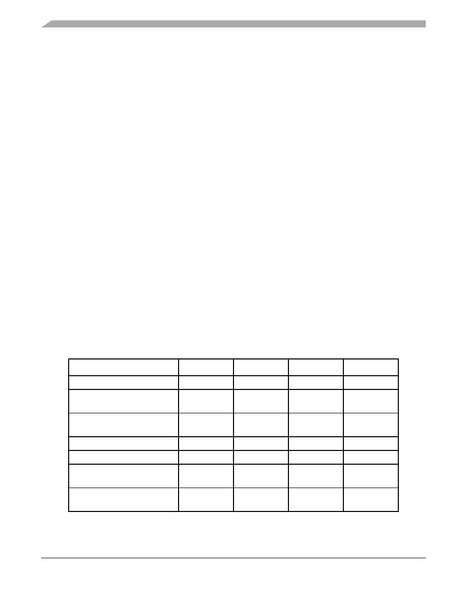
Table 21. GMII, MII, and TBI DC Electrical Characteristics
Parameter
Symbol
Min
Max
Unit
Supply voltage 3.3 V
LVDD
3.13
3.47
V
Output high voltage
(LVDD = Min, IOH = –4.0 mA)
VOH
2.40
LVDD + 0.3
V
Output low voltage
(LVDD = Min, IOL = 4.0 mA)
VOL
GND
0.50
V
Input high voltage
VIH
1.70
LVDD + 0.3
V
Input low voltage
VIL
–0.3
0.90
V
Input high current
(VIN
1 = LV
DD)
IIH
—40
μA
Input low current
(VIN
1 = GND)
IIL
–600
—
μA
Note:
相关PDF资料 |
PDF描述 |
|---|---|
| MPC8541VTAQF | IC MPU POWERQUICC III 783-FCPBGA |
| MPC8544EAVTARJA | IC MPU POWERQUICC III 783-FCBGA |
| MPC8548ECVTAQGB | MPU POWERQUICC III 783-PBGA |
| MPC8555VTAQF | IC MPU POWERQUICC III 783-FCPBGA |
| MPC855TCVR66D4 | IC MPU POWERQUICC 66MHZ 357-PBGA |
相关代理商/技术参数 |
参数描述 |
|---|---|
| MPC8541CPXAJD | 功能描述:微处理器 - MPU PQ 37 LITE 8555 RoHS:否 制造商:Atmel 处理器系列:SAMA5D31 核心:ARM Cortex A5 数据总线宽度:32 bit 最大时钟频率:536 MHz 程序存储器大小:32 KB 数据 RAM 大小:128 KB 接口类型:CAN, Ethernet, LIN, SPI,TWI, UART, USB 工作电源电压:1.8 V to 3.3 V 最大工作温度:+ 85 C 安装风格:SMD/SMT 封装 / 箱体:FBGA-324 |
| MPC8541CVTAJD | 功能描述:微处理器 - MPU PQ 37 LITE 8555 RoHS:否 制造商:Atmel 处理器系列:SAMA5D31 核心:ARM Cortex A5 数据总线宽度:32 bit 最大时钟频率:536 MHz 程序存储器大小:32 KB 数据 RAM 大小:128 KB 接口类型:CAN, Ethernet, LIN, SPI,TWI, UART, USB 工作电源电压:1.8 V to 3.3 V 最大工作温度:+ 85 C 安装风格:SMD/SMT 封装 / 箱体:FBGA-324 |
| MPC8541E PXAJD | 制造商:FREESCALE-SEMI 功能描述: |
| MPC8541ECPXAJD | 功能描述:微处理器 - MPU PQ 37 LITE 8555E RoHS:否 制造商:Atmel 处理器系列:SAMA5D31 核心:ARM Cortex A5 数据总线宽度:32 bit 最大时钟频率:536 MHz 程序存储器大小:32 KB 数据 RAM 大小:128 KB 接口类型:CAN, Ethernet, LIN, SPI,TWI, UART, USB 工作电源电压:1.8 V to 3.3 V 最大工作温度:+ 85 C 安装风格:SMD/SMT 封装 / 箱体:FBGA-324 |
| MPC8541ECPXALF | 功能描述:微处理器 - MPU PQ 37 LITE 8555E RoHS:否 制造商:Atmel 处理器系列:SAMA5D31 核心:ARM Cortex A5 数据总线宽度:32 bit 最大时钟频率:536 MHz 程序存储器大小:32 KB 数据 RAM 大小:128 KB 接口类型:CAN, Ethernet, LIN, SPI,TWI, UART, USB 工作电源电压:1.8 V to 3.3 V 最大工作温度:+ 85 C 安装风格:SMD/SMT 封装 / 箱体:FBGA-324 |
发布紧急采购,3分钟左右您将得到回复。