- 您现在的位置:买卖IC网 > PDF目录1955 > MPC8540VTAQFC (Freescale Semiconductor)MPU POWERQUICC III 783FCPBGA PDF资料下载
参数资料
| 型号: | MPC8540VTAQFC |
| 厂商: | Freescale Semiconductor |
| 文件页数: | 65/104页 |
| 文件大小: | 0K |
| 描述: | MPU POWERQUICC III 783FCPBGA |
| 标准包装: | 36 |
| 系列: | MPC85xx |
| 处理器类型: | 32-位 MPC85xx PowerQUICC III |
| 速度: | 1.0GHz |
| 电压: | 1.3V |
| 安装类型: | 表面贴装 |
| 封装/外壳: | 784-BBGA,FCBGA |
| 供应商设备封装: | 783-FCPBGA(29x29) |
| 包装: | 托盘 |
第1页第2页第3页第4页第5页第6页第7页第8页第9页第10页第11页第12页第13页第14页第15页第16页第17页第18页第19页第20页第21页第22页第23页第24页第25页第26页第27页第28页第29页第30页第31页第32页第33页第34页第35页第36页第37页第38页第39页第40页第41页第42页第43页第44页第45页第46页第47页第48页第49页第50页第51页第52页第53页第54页第55页第56页第57页第58页第59页第60页第61页第62页第63页第64页当前第65页第66页第67页第68页第69页第70页第71页第72页第73页第74页第75页第76页第77页第78页第79页第80页第81页第82页第83页第84页第85页第86页第87页第88页第89页第90页第91页第92页第93页第94页第95页第96页第97页第98页第99页第100页第101页第102页第103页第104页
MPC8540 Integrated Processor Hardware Specifications, Rev. 4.1
Freescale Semiconductor
63
RapidIO
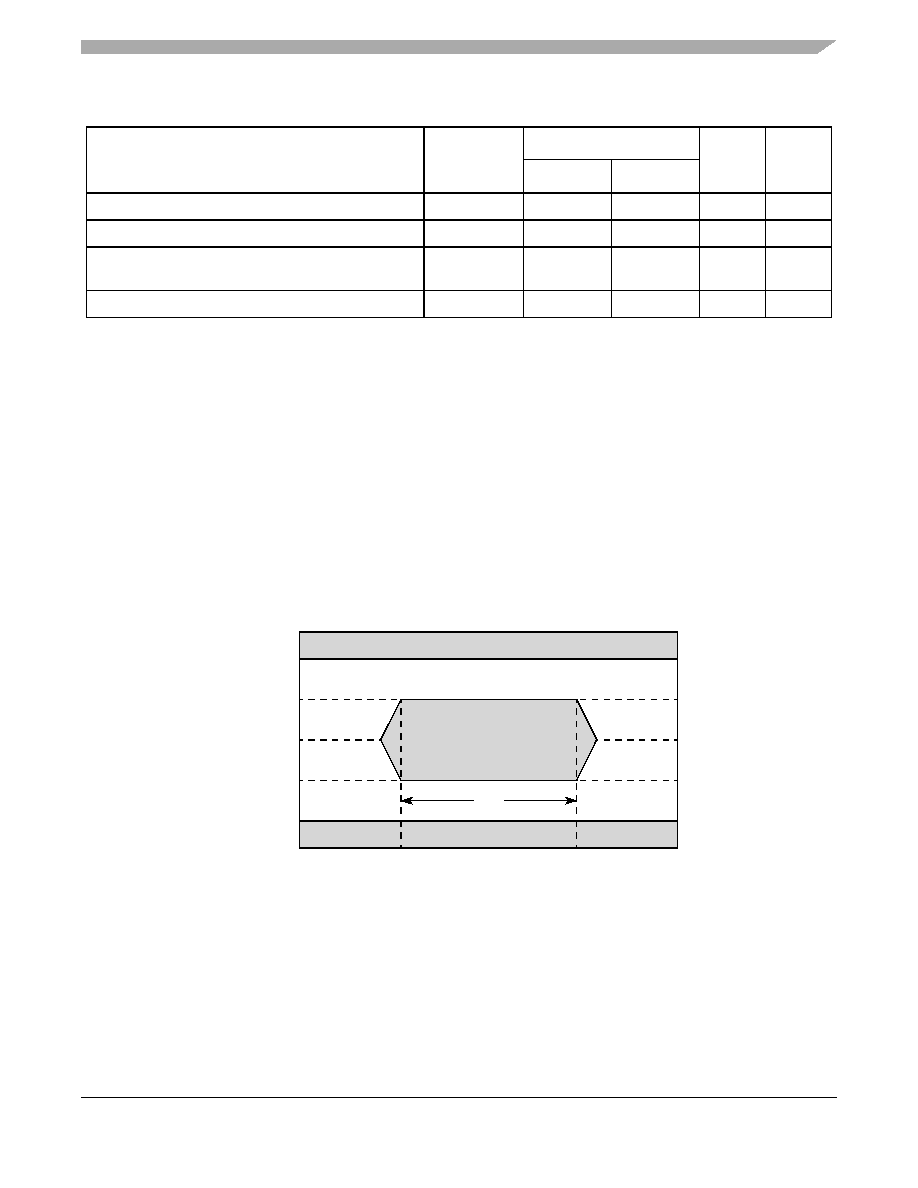
The compliance of receiver input signals RD[0:15] and RFRAME with their minimum data valid window
(DV) specification shall be determined by generating an eye pattern for each of the data signals and
comparing the eye pattern of each data signal with the RapidIO receive mask shown in Figure 40. The
value of X2 used to construct the mask shall be (1 – DVmin)/2. The ±100 mV minimum data valid and
±600 mV maximum input voltage values are from the DC specification. A signal is compliant with the data
valid window specification if and only if the receive mask can be positioned on the signal’s eye pattern
such that the eye pattern falls entirely within the unshaded portion of the mask.
Figure 40. RapidIO Receive Mask
The eye pattern for a data signal is generated by making a large number of recordings of the signal and
then overlaying the recordings. The number of recordings used to generate the eye shall be large enough
that further increasing the number of recordings used does not cause the resulting eye pattern to change
from one that complies with the RapidIO receive mask to one that does not. Each data signal in the
interface shall be carrying random or pseudo-random data when the recordings are made. If
pseudo-random data is used, the length of the pseudo-random sequence (repeat length) shall be long
Table 52. RapidIO Receiver AC Timing Specifications—1 Gbps Data Rate
Characteristic
Symbol
Range
Unit
Notes
Min
Max
Duty cycle of the clock input
DC
47
53
%
1, 5
Data valid
DV
425
—
ps
2
Allowable static skew between any two data inputs
within a 8-/9-bit group
tDPAIR
—
300
ps
3
Allowable static skew of data inputs to associated clock
tSKEW,PAIR
–200
200
ps
4
Notes:
1.Measured at VID = 0 V.
2.Measured using the RapidIO receive mask shown in Figure 40.
3.See Figure 43.
4.See Figure 42 and Figure 43.
5.Guaranteed by design.
X2
600
0
100
–100
–600
1–X2
DV
V
ID
(m
V)
Time (UI)
01
相关PDF资料 |
PDF描述 |
|---|---|
| MPC8541VTAQF | IC MPU POWERQUICC III 783-FCPBGA |
| MPC8544EAVTARJA | IC MPU POWERQUICC III 783-FCBGA |
| MPC8548ECVTAQGB | MPU POWERQUICC III 783-PBGA |
| MPC8555VTAQF | IC MPU POWERQUICC III 783-FCPBGA |
| MPC855TCVR66D4 | IC MPU POWERQUICC 66MHZ 357-PBGA |
相关代理商/技术参数 |
参数描述 |
|---|---|
| MPC8541CPXAJD | 功能描述:微处理器 - MPU PQ 37 LITE 8555 RoHS:否 制造商:Atmel 处理器系列:SAMA5D31 核心:ARM Cortex A5 数据总线宽度:32 bit 最大时钟频率:536 MHz 程序存储器大小:32 KB 数据 RAM 大小:128 KB 接口类型:CAN, Ethernet, LIN, SPI,TWI, UART, USB 工作电源电压:1.8 V to 3.3 V 最大工作温度:+ 85 C 安装风格:SMD/SMT 封装 / 箱体:FBGA-324 |
| MPC8541CVTAJD | 功能描述:微处理器 - MPU PQ 37 LITE 8555 RoHS:否 制造商:Atmel 处理器系列:SAMA5D31 核心:ARM Cortex A5 数据总线宽度:32 bit 最大时钟频率:536 MHz 程序存储器大小:32 KB 数据 RAM 大小:128 KB 接口类型:CAN, Ethernet, LIN, SPI,TWI, UART, USB 工作电源电压:1.8 V to 3.3 V 最大工作温度:+ 85 C 安装风格:SMD/SMT 封装 / 箱体:FBGA-324 |
| MPC8541E PXAJD | 制造商:FREESCALE-SEMI 功能描述: |
| MPC8541ECPXAJD | 功能描述:微处理器 - MPU PQ 37 LITE 8555E RoHS:否 制造商:Atmel 处理器系列:SAMA5D31 核心:ARM Cortex A5 数据总线宽度:32 bit 最大时钟频率:536 MHz 程序存储器大小:32 KB 数据 RAM 大小:128 KB 接口类型:CAN, Ethernet, LIN, SPI,TWI, UART, USB 工作电源电压:1.8 V to 3.3 V 最大工作温度:+ 85 C 安装风格:SMD/SMT 封装 / 箱体:FBGA-324 |
| MPC8541ECPXALF | 功能描述:微处理器 - MPU PQ 37 LITE 8555E RoHS:否 制造商:Atmel 处理器系列:SAMA5D31 核心:ARM Cortex A5 数据总线宽度:32 bit 最大时钟频率:536 MHz 程序存储器大小:32 KB 数据 RAM 大小:128 KB 接口类型:CAN, Ethernet, LIN, SPI,TWI, UART, USB 工作电源电压:1.8 V to 3.3 V 最大工作温度:+ 85 C 安装风格:SMD/SMT 封装 / 箱体:FBGA-324 |
发布紧急采购,3分钟左右您将得到回复。