- 您现在的位置:买卖IC网 > PDF目录2099 > MPC9772FA (IDT, Integrated Device Technology Inc)IC PLL CLK GEN 1:12 3.3V 52-LQFP PDF资料下载
参数资料
| 型号: | MPC9772FA |
| 厂商: | IDT, Integrated Device Technology Inc |
| 文件页数: | 12/17页 |
| 文件大小: | 0K |
| 描述: | IC PLL CLK GEN 1:12 3.3V 52-LQFP |
| 标准包装: | 160 |
| 类型: | PLL 时钟发生器 |
| PLL: | 带旁路 |
| 输入: | LVCMOS,晶体 |
| 输出: | LVCMOS |
| 电路数: | 1 |
| 比率 - 输入:输出: | 3:12 |
| 差分 - 输入:输出: | 无/无 |
| 频率 - 最大: | 240MHz |
| 除法器/乘法器: | 是/无 |
| 电源电压: | 3.135 V ~ 3.465 V |
| 工作温度: | 0°C ~ 70°C |
| 安装类型: | 表面贴装 |
| 封装/外壳: | 52-LQFP |
| 供应商设备封装: | 52-TQFP(10x10) |
| 包装: | 托盘 |
MPC9772 REVISION 7 JANUARY 8, 2013
4
2013 Integrated Device Technology, Inc.
MPC9772 Data Sheet
3.3V 1:12 LVCMOS PLL CLOCK GENERATOR
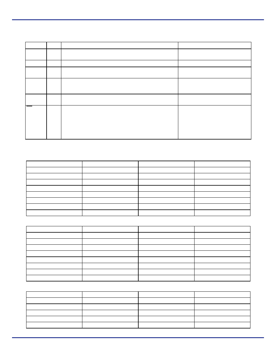
Table 2. Function Table (Configuration Controls)
Control
Default
0
1
REF_SEL
1
Selects CCLKx as the PLL reference clock
Selects the crystal oscillator as the PLL
reference clock
CCLK_SEL
1
Selects CCLK0
Selects CCLK1
VCO_SEL
1
Selects VCO
2. The VCO frequency is scaled by a factor of 2 (low VCO
frequency range).
Selects VCO
1. (high VCO frequency range)
PLL_EN
1
Test mode with the PLL bypassed. The reference clock is substituted for the
internal VCO output. MPC9772 is fully static and no minimum frequency
limit applies. All PLL related AC characteristics are not applicable.
Normal operation mode with PLL enabled.
INV_CLK
1
QC2 and QC3 are in phase with QC0 and QC1
QC2 and QC3 are inverted (180
phase shift)
with respect to QC0 and QC1
MR/OE
1
Outputs disabled (high-impedance state) and device is reset. During
reset/output disable the PLL feedback loop is open and the internal VCO
is tied to its lowest frequency. The MPC9772 requires reset after any loss
of PLL lock. Loss of PLL lock may occur when the external feedback path
is interrupted. The length of the reset pulse should be greater than one
reference clock cycle (CCLKx). The device is reset by the internal power-
on reset (POR) circuitry during power-up.
Outputs enabled (active)
VCO_SEL, FSEL_A[0:1], FSEL_B[0:1], FSEL_C[0:1], FSEL_FB[0:2] control the operating PLL frequency range and input/output frequency
ratios. See Table 3 to Table 6 and the Applications Information for supported frequency ranges and output to input frequency ratios.
Table 3. Output Divider Bank A (NA)
VCO_SEL
FSEL_A1
FSEL_A0
QA[0:3]
0
VCO
8
0
1
VCO
12
0
1
0
VCO
16
0
1
VCO
24
1
0
VCO
4
1
0
1
VCO
6
1
0
VCO
8
1
VCO
12
Table 4. Output Divider Bank B (NB)
VCO_SEL
FSEL_B1
FSEL_B0
QB[0:3]
0
VCO
8
0
1
VCO
12
0
1
0
VCO
16
0
1
VCO
20
1
0
VCO
4
1
0
1
VCO
6
1
0
VCO
8
1
VCO
10
Table 5. Output Divider Bank C (NC)
VCO_SEL
FSEL_C1
FSEL_C0
QC[0:3]
0
VCO
4
0
1
VCO
8
0
1
0
VCO
12
0
1
VCO
16
1
0
VCO
2
相关PDF资料 |
PDF描述 |
|---|---|
| MPC9774FAR2 | IC PLL CLK GEN 1:14 3.3V 52-LQFP |
| MPC97H74AE | IC PLL CLK GEN 1:14 3.3V 52-LQFP |
| MPC9993AC | IC PLL CLK DRIVER IDCS 32-LQFP |
| MPC99J93AC | IC PLL CLK DRIVER IDCS 32-LQFP |
| MPR032EPR2 | IC CTLR TOUCH SENSOR 8-DFN |
相关代理商/技术参数 |
参数描述 |
|---|---|
| MPC9772FAR2 | 功能描述:时钟发生器及支持产品 FSL 1-12 LVCMOS PLL Clock Generator, xta RoHS:否 制造商:Silicon Labs 类型:Clock Generators 最大输入频率:14.318 MHz 最大输出频率:166 MHz 输出端数量:16 占空比 - 最大:55 % 工作电源电压:3.3 V 工作电源电流:1 mA 最大工作温度:+ 85 C 安装风格:SMD/SMT 封装 / 箱体:QFN-56 |
| MPC9773 | 制造商:FREESCALE 制造商全称:Freescale Semiconductor, Inc 功能描述:3.3 V 1:12 LVCMOS PLL Clock Generator |
| MPC9773AE | 功能描述:时钟发生器及支持产品 FSL 1-12 LVCMOS/LVPE CL to LVCMOS PLL Clo RoHS:否 制造商:Silicon Labs 类型:Clock Generators 最大输入频率:14.318 MHz 最大输出频率:166 MHz 输出端数量:16 占空比 - 最大:55 % 工作电源电压:3.3 V 工作电源电流:1 mA 最大工作温度:+ 85 C 安装风格:SMD/SMT 封装 / 箱体:QFN-56 |
| MPC9773AER2 | 功能描述:时钟发生器及支持产品 FSL 1-12 LVCMOS/LVPE CL to LVCMOS PLL Clo RoHS:否 制造商:Silicon Labs 类型:Clock Generators 最大输入频率:14.318 MHz 最大输出频率:166 MHz 输出端数量:16 占空比 - 最大:55 % 工作电源电压:3.3 V 工作电源电流:1 mA 最大工作温度:+ 85 C 安装风格:SMD/SMT 封装 / 箱体:QFN-56 |
| MPC9773FA | 功能描述:锁相环 - PLL 3.3V 240MHz Clock Generator RoHS:否 制造商:Silicon Labs 类型:PLL Clock Multiplier 电路数量:1 最大输入频率:710 MHz 最小输入频率:0.002 MHz 输出频率范围:0.002 MHz to 808 MHz 电源电压-最大:3.63 V 电源电压-最小:1.71 V 最大工作温度:+ 85 C 最小工作温度:- 40 C 封装 / 箱体:QFN-36 封装:Tray |
发布紧急采购,3分钟左右您将得到回复。