- 您现在的位置:买卖IC网 > PDF目录2099 > MPC9772FA (IDT, Integrated Device Technology Inc)IC PLL CLK GEN 1:12 3.3V 52-LQFP PDF资料下载
参数资料
| 型号: | MPC9772FA |
| 厂商: | IDT, Integrated Device Technology Inc |
| 文件页数: | 17/17页 |
| 文件大小: | 0K |
| 描述: | IC PLL CLK GEN 1:12 3.3V 52-LQFP |
| 标准包装: | 160 |
| 类型: | PLL 时钟发生器 |
| PLL: | 带旁路 |
| 输入: | LVCMOS,晶体 |
| 输出: | LVCMOS |
| 电路数: | 1 |
| 比率 - 输入:输出: | 3:12 |
| 差分 - 输入:输出: | 无/无 |
| 频率 - 最大: | 240MHz |
| 除法器/乘法器: | 是/无 |
| 电源电压: | 3.135 V ~ 3.465 V |
| 工作温度: | 0°C ~ 70°C |
| 安装类型: | 表面贴装 |
| 封装/外壳: | 52-LQFP |
| 供应商设备封装: | 52-TQFP(10x10) |
| 包装: | 托盘 |
MPC9772 REVISION 7 JANUARY 8, 2013
9
2013 Integrated Device Technology, Inc.
MPC9772 Data Sheet
3.3V 1:12 LVCMOS PLL CLOCK GENERATOR
MPC9772 Individual Output Disable
(Clock Stop) Circuitry
The individual clock stop (output enable) control of the
MPC9772 allows designers, under software control, to
implement power management into the clock distribution
design. A simple serial interface and a clock stop control logic
provides a mechanism through which the MPC9772 clock
outputs can be individually stopped in the logic ‘0’ state: The
clock stop mechanism allows serial loading of a 12-bit serial
input register. This register contains one programmable clock
stop bit for 12 of the 14 output clocks. The QC0 and QFB
outputs cannot be stopped (disabled) with the serial port.
The user can program an output clock to stop (disable) by
writing logic ‘0’ to the respective stop enable bit. Likewise, the
user may programmably enable an output clock by writing
logic ‘1’ to the respective enable bit. The clock stop logic
enables or disables clock outputs during the time when the
output would be in normally in logic low state, eliminating the
possibility of short or ‘runt’ clock pulses.
The user can write to the serial input register through the
STOP_DATA input by supplying a logic ‘0’ start bit followed
serially by 12 NRZ disable/enable bits. The period of each
STOP_DATA bit equals the period of the free—running
STOP_CLK signal. The STOP_DATA serial transmission
should be timed so the MPC9772 can sample each
STOP_DATA bit with the rising edge of the free—running
STOP_CLK signal. (See Figure 5.)
SYNC Output Description
The MPC9772 has a system synchronization pulse output
QSYNC. In configurations with the output frequency
relationships are not integer multiples of each other QSYNC
provides a signal for system synchronization purposes. The
MPC9772 monitors the relationship between the A bank and
the B bank of outputs. The QSYNC output is asserted (logic
low) one period in duration and one period prior to the
coincident rising edges of the QA and QC outputs. The
duration and the placement of the pulse is dependent QA and
QC output frequencies: the QSYNC pulse width is equal to
the period of the higher of the QA and QC output frequencies.
Figure 6 shows various waveforms for the QSYNC output.
The QSYNC output is defined for all possible combinations of
the bank A and bank C outputs.
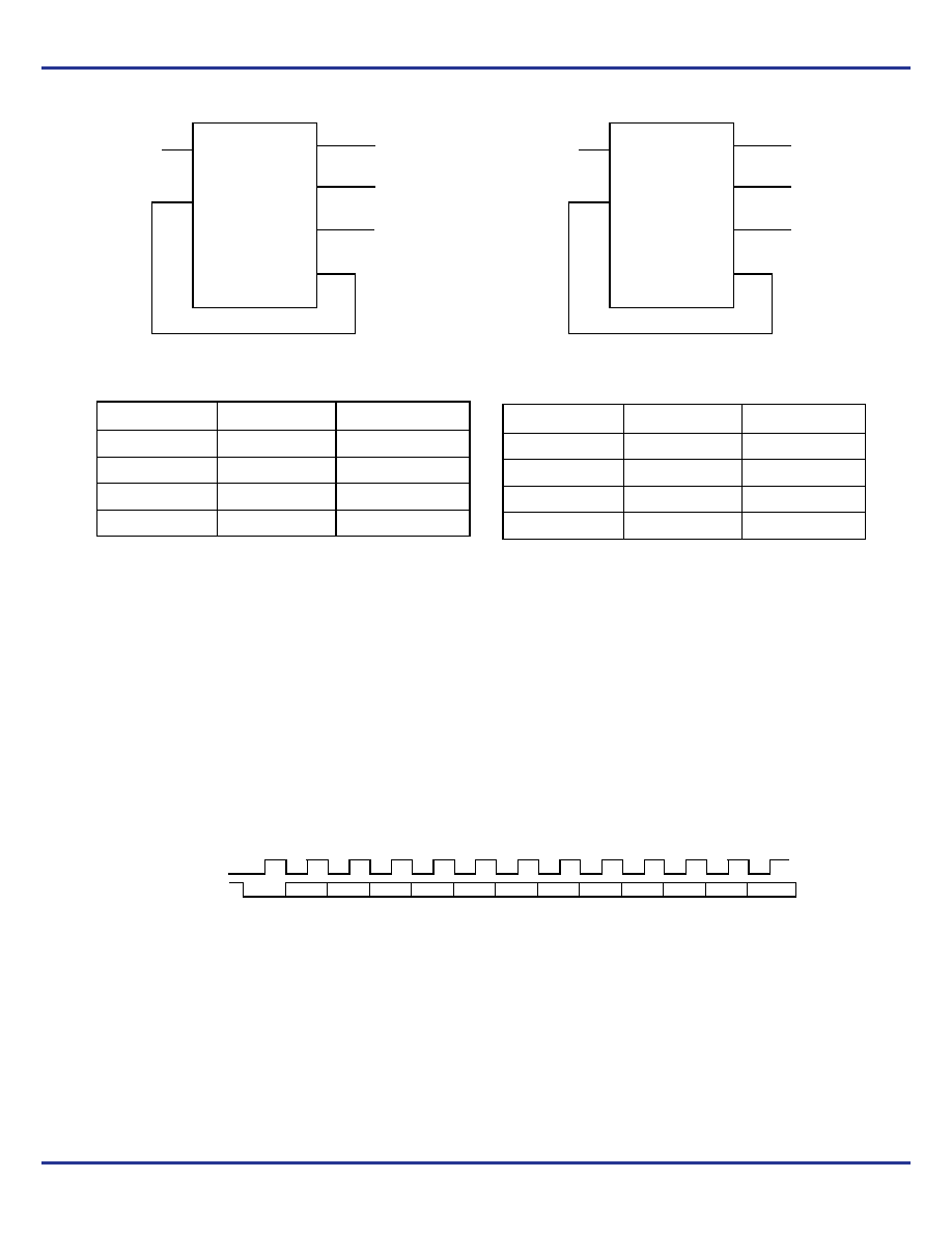
Figure 3. Example Configuration
Figure 4. Example Configuration
MPC9772
fref = 33.3 MHz
33.3 MHz
100 MHz
33.3 MHz (Feedback)
200 MHz
CCLK0
VCO_SEL
FSEL_A[1:0]
FSEL_B[1:0]
FSEL_C[1:0]
FSEL_FB[2:0]
QA[3:0]
QB[3:0]
QC[3:0]
QFB
CCLK1
CCLK_SEL
FB_IN
1
11
00
101
MPC9772 example configuration (feedback of QFB = 33.3 MHz,
fVCO=400 MHz, VCO_SEL=1, M=12, NA=12, NB=4, NC=2).
Frequency Range
TA = 0°C to +70°C TA = –40°C to +85°C
Input
16.6 – 40 MHz
16.6 – 38.33 MHz
QA Outputs
16.6 – 40 MHz
16.6 – 38.33 MHz
QA Outputs
50 – 120 MHz
50 – 115 MHz
QC Outputs
100 – 240 MHz
100 – 230 MHz
MPC9772
fref = 25 MHz
62.5 MHz
25 MHz (Feedback)
125 MHz
CCLK0
VCO_SEL
FSEL_A[1:0]
FSEL_B[1:0]
FSEL_C[1:0]
FSEL_FB[2:0]
QA[3:0]
QB[3:0]
QC[3:0]
QFB
CCLK1
CCLK_SEL
FB_IN
1
00
011
MPC9772 example configuration (feedback of QFB = 25 MHz,
fVCO=250 MHz, VCO_SEL=1, M=10, NA=4, NB=4, NC=2).
Frequency Range
TA = 0°C to +70°C TA = –40°C to +85°C
Input
20 – 48 MHz
20 – 46 MHz
QA Outputs
50 – 120 MHz
50 – 115 MHz
QA Outputs
50 – 120 MHz
50 – 115 MHz
QC Outputs
100 – 240 MHz
100 – 230 MHz
Figure 5. Clock Stop Circuit Programming
STOP_CLK
STOP_DATA
START
QA0
QA1
QA2
QA3
QB0
QB1
QB2
QB3
QC1
QC2
QC3
QSYNC
相关PDF资料 |
PDF描述 |
|---|---|
| MPC9774FAR2 | IC PLL CLK GEN 1:14 3.3V 52-LQFP |
| MPC97H74AE | IC PLL CLK GEN 1:14 3.3V 52-LQFP |
| MPC9993AC | IC PLL CLK DRIVER IDCS 32-LQFP |
| MPC99J93AC | IC PLL CLK DRIVER IDCS 32-LQFP |
| MPR032EPR2 | IC CTLR TOUCH SENSOR 8-DFN |
相关代理商/技术参数 |
参数描述 |
|---|---|
| MPC9772FAR2 | 功能描述:时钟发生器及支持产品 FSL 1-12 LVCMOS PLL Clock Generator, xta RoHS:否 制造商:Silicon Labs 类型:Clock Generators 最大输入频率:14.318 MHz 最大输出频率:166 MHz 输出端数量:16 占空比 - 最大:55 % 工作电源电压:3.3 V 工作电源电流:1 mA 最大工作温度:+ 85 C 安装风格:SMD/SMT 封装 / 箱体:QFN-56 |
| MPC9773 | 制造商:FREESCALE 制造商全称:Freescale Semiconductor, Inc 功能描述:3.3 V 1:12 LVCMOS PLL Clock Generator |
| MPC9773AE | 功能描述:时钟发生器及支持产品 FSL 1-12 LVCMOS/LVPE CL to LVCMOS PLL Clo RoHS:否 制造商:Silicon Labs 类型:Clock Generators 最大输入频率:14.318 MHz 最大输出频率:166 MHz 输出端数量:16 占空比 - 最大:55 % 工作电源电压:3.3 V 工作电源电流:1 mA 最大工作温度:+ 85 C 安装风格:SMD/SMT 封装 / 箱体:QFN-56 |
| MPC9773AER2 | 功能描述:时钟发生器及支持产品 FSL 1-12 LVCMOS/LVPE CL to LVCMOS PLL Clo RoHS:否 制造商:Silicon Labs 类型:Clock Generators 最大输入频率:14.318 MHz 最大输出频率:166 MHz 输出端数量:16 占空比 - 最大:55 % 工作电源电压:3.3 V 工作电源电流:1 mA 最大工作温度:+ 85 C 安装风格:SMD/SMT 封装 / 箱体:QFN-56 |
| MPC9773FA | 功能描述:锁相环 - PLL 3.3V 240MHz Clock Generator RoHS:否 制造商:Silicon Labs 类型:PLL Clock Multiplier 电路数量:1 最大输入频率:710 MHz 最小输入频率:0.002 MHz 输出频率范围:0.002 MHz to 808 MHz 电源电压-最大:3.63 V 电源电压-最小:1.71 V 最大工作温度:+ 85 C 最小工作温度:- 40 C 封装 / 箱体:QFN-36 封装:Tray |
发布紧急采购,3分钟左右您将得到回复。