- 您现在的位置:买卖IC网 > PDF目录2099 > MPC9772FA (IDT, Integrated Device Technology Inc)IC PLL CLK GEN 1:12 3.3V 52-LQFP PDF资料下载
参数资料
| 型号: | MPC9772FA |
| 厂商: | IDT, Integrated Device Technology Inc |
| 文件页数: | 4/17页 |
| 文件大小: | 0K |
| 描述: | IC PLL CLK GEN 1:12 3.3V 52-LQFP |
| 标准包装: | 160 |
| 类型: | PLL 时钟发生器 |
| PLL: | 带旁路 |
| 输入: | LVCMOS,晶体 |
| 输出: | LVCMOS |
| 电路数: | 1 |
| 比率 - 输入:输出: | 3:12 |
| 差分 - 输入:输出: | 无/无 |
| 频率 - 最大: | 240MHz |
| 除法器/乘法器: | 是/无 |
| 电源电压: | 3.135 V ~ 3.465 V |
| 工作温度: | 0°C ~ 70°C |
| 安装类型: | 表面贴装 |
| 封装/外壳: | 52-LQFP |
| 供应商设备封装: | 52-TQFP(10x10) |
| 包装: | 托盘 |
MPC9772 REVISION 7 JANUARY 8, 2013
12
2013 Integrated Device Technology, Inc.
MPC9772 Data Sheet
3.3V 1:12 LVCMOS PLL CLOCK GENERATOR
(CF) can be derived from Table 12.
The feedback trace delay is determined by the board
layout and can be used to fine-tune the effective delay
through each device.
Due to the frequency dependence of the static phase
maximum I/O jitter and the specified t( parameter relative to
the input reference frequency results in a precise timing
performance analysis.
In the following example calculation an I/O jitter confidence
factor of 99.7% (
3) is assumed, resulting in a worst case
timing uncertainty from the common input reference clock to
any output of –455 ps to +455 ps relative to CCLK (PLL
feedback =
8, reference frequency = 50 MHz, VCO
frequency = 400 MHz, I/O jitter = 13 ps rms max., static
phase offset t() = 166 ps):
tSK(PP) = [-166ps...166ps] + [-250ps...250ps] +
[(13ps @ –3)...(13ps @ 3)] + tPD, LINE(FB)
tSK(PP) = [-455ps...455ps] + tPD, LINE(FB)
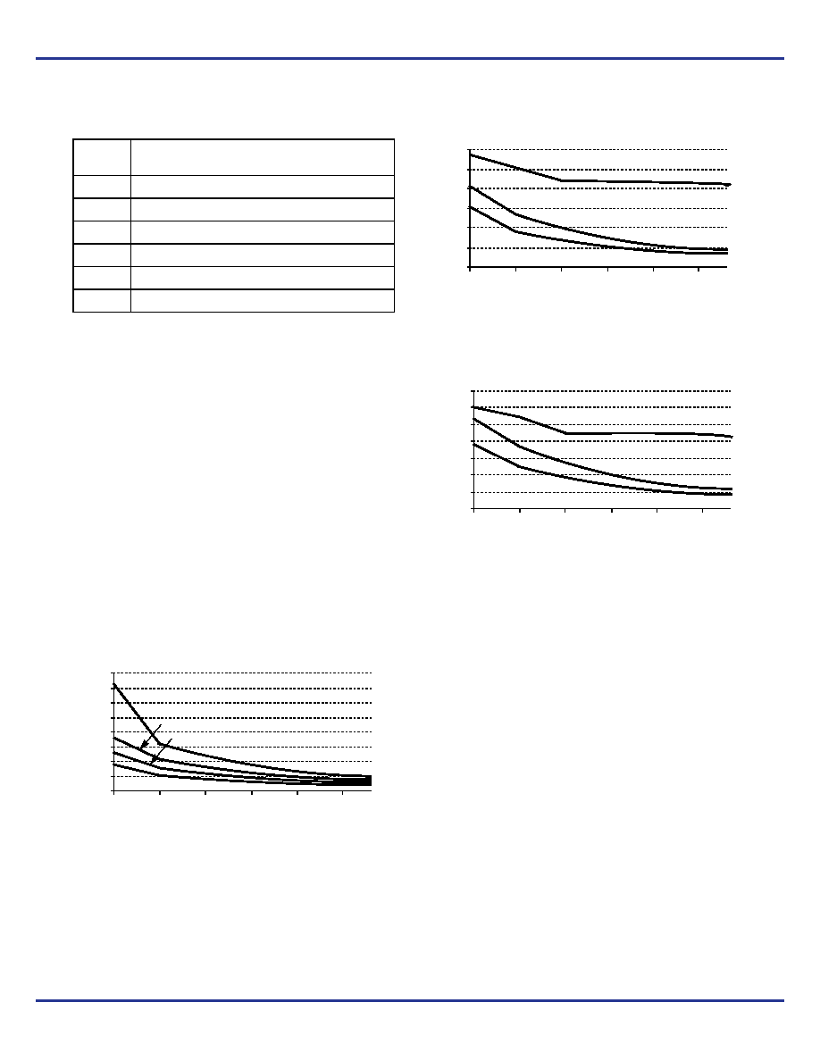
Figure 9. MPC9772 I/O Jitter
Figure 10. MPC9772 I/O Jitter
Figure 11. MPC9772 I/O Jitter
Driving Transmission Lines
The MPC9772 clock driver was designed to drive high
speed signals in a terminated transmission line environment.
To provide the optimum flexibility to the user the output
drivers were designed to exhibit the lowest impedance
possible. With an output impedance of less than 20
the
drivers can drive either parallel or series terminated
transmission lines. For more information on transmission
lines the reader is referred to Freescale Semiconductor
application note AN1091. In most high performance clock
networks point-to-point distribution of signals is the method of
choice. In a point-to-point scheme either series terminated or
parallel terminated transmission lines can be used. The
parallel technique terminates the signal at the end of the line
with a 50
resistance to VCC2.
This technique draws a fairly high level of DC current and
thus only a single terminated line can be driven by each
output of the MPC9772 clock driver. For the series terminated
case however there is no DC current draw, thus the outputs
can drive multiple series terminated lines. Figure 12
illustrates an output driving a single series terminated line
versus two series terminated lines in parallel. When taken to
its extreme the fanout of the MPC9772 clock driver is
effectively doubled due to its capability to drive multiple lines.
Table 12. Confidence Factor CF
CF
Probability of Clock Edge
within the Distribution
1
0.68268948
2
0.95449988
3
0.99730007
4
0.99993663
5
0.99999943
6
0.99999999
VCO Frequency [MHz]
200
250
300
350
400
450
480
160
140
120
100
80
60
40
20
0
FB=
32
FB=
16
FB=
8
FB=
4
Max. I/O Phase Jitter versus Frequency
Parameter: PLL Feedback Divider FB
t jit(
)[p
s]
RMS
VCO Frequency [MHz]
200
250
300
350
400
450
480
120
100
80
60
40
20
0
FB=
12
FB=
24
Max. I/O Phase Jitter versus Frequency
Parameter: PLL Feedback Divider FB
FB=
6
t jit(
)[p
s]
RMS
VCO Frequency [MHz]
200
250
300
350
400
450
480
140
120
100
80
60
40
20
0
FB=
20
FB=
10
FB=
40
Max. I/O Phase Jitter versus Frequency
Parameter: PLL Feedback Divider FB
t jit(
)[p
s]
RMS
相关PDF资料 |
PDF描述 |
|---|---|
| MPC9774FAR2 | IC PLL CLK GEN 1:14 3.3V 52-LQFP |
| MPC97H74AE | IC PLL CLK GEN 1:14 3.3V 52-LQFP |
| MPC9993AC | IC PLL CLK DRIVER IDCS 32-LQFP |
| MPC99J93AC | IC PLL CLK DRIVER IDCS 32-LQFP |
| MPR032EPR2 | IC CTLR TOUCH SENSOR 8-DFN |
相关代理商/技术参数 |
参数描述 |
|---|---|
| MPC9772FAR2 | 功能描述:时钟发生器及支持产品 FSL 1-12 LVCMOS PLL Clock Generator, xta RoHS:否 制造商:Silicon Labs 类型:Clock Generators 最大输入频率:14.318 MHz 最大输出频率:166 MHz 输出端数量:16 占空比 - 最大:55 % 工作电源电压:3.3 V 工作电源电流:1 mA 最大工作温度:+ 85 C 安装风格:SMD/SMT 封装 / 箱体:QFN-56 |
| MPC9773 | 制造商:FREESCALE 制造商全称:Freescale Semiconductor, Inc 功能描述:3.3 V 1:12 LVCMOS PLL Clock Generator |
| MPC9773AE | 功能描述:时钟发生器及支持产品 FSL 1-12 LVCMOS/LVPE CL to LVCMOS PLL Clo RoHS:否 制造商:Silicon Labs 类型:Clock Generators 最大输入频率:14.318 MHz 最大输出频率:166 MHz 输出端数量:16 占空比 - 最大:55 % 工作电源电压:3.3 V 工作电源电流:1 mA 最大工作温度:+ 85 C 安装风格:SMD/SMT 封装 / 箱体:QFN-56 |
| MPC9773AER2 | 功能描述:时钟发生器及支持产品 FSL 1-12 LVCMOS/LVPE CL to LVCMOS PLL Clo RoHS:否 制造商:Silicon Labs 类型:Clock Generators 最大输入频率:14.318 MHz 最大输出频率:166 MHz 输出端数量:16 占空比 - 最大:55 % 工作电源电压:3.3 V 工作电源电流:1 mA 最大工作温度:+ 85 C 安装风格:SMD/SMT 封装 / 箱体:QFN-56 |
| MPC9773FA | 功能描述:锁相环 - PLL 3.3V 240MHz Clock Generator RoHS:否 制造商:Silicon Labs 类型:PLL Clock Multiplier 电路数量:1 最大输入频率:710 MHz 最小输入频率:0.002 MHz 输出频率范围:0.002 MHz to 808 MHz 电源电压-最大:3.63 V 电源电压-最小:1.71 V 最大工作温度:+ 85 C 最小工作温度:- 40 C 封装 / 箱体:QFN-36 封装:Tray |
发布紧急采购,3分钟左右您将得到回复。