- 您现在的位置:买卖IC网 > PDF目录2099 > MPC9772FA (IDT, Integrated Device Technology Inc)IC PLL CLK GEN 1:12 3.3V 52-LQFP PDF资料下载
参数资料
| 型号: | MPC9772FA |
| 厂商: | IDT, Integrated Device Technology Inc |
| 文件页数: | 3/17页 |
| 文件大小: | 0K |
| 描述: | IC PLL CLK GEN 1:12 3.3V 52-LQFP |
| 标准包装: | 160 |
| 类型: | PLL 时钟发生器 |
| PLL: | 带旁路 |
| 输入: | LVCMOS,晶体 |
| 输出: | LVCMOS |
| 电路数: | 1 |
| 比率 - 输入:输出: | 3:12 |
| 差分 - 输入:输出: | 无/无 |
| 频率 - 最大: | 240MHz |
| 除法器/乘法器: | 是/无 |
| 电源电压: | 3.135 V ~ 3.465 V |
| 工作温度: | 0°C ~ 70°C |
| 安装类型: | 表面贴装 |
| 封装/外壳: | 52-LQFP |
| 供应商设备封装: | 52-TQFP(10x10) |
| 包装: | 托盘 |
MPC9772 REVISION 7 JANUARY 8, 2013
11
2013 Integrated Device Technology, Inc.
MPC9772 Data Sheet
3.3V 1:12 LVCMOS PLL CLOCK GENERATOR
Power Supply Filtering
The MPC9772 is a mixed analog/digital product. Its analog
circuitry is naturally susceptible to random noise, especially if
this noise is seen on the power supply pins. Random noise
on the VCC_PLL power supply impacts the device
characteristics, for instance I/O jitter. The MPC9772 provides
separate power supplies for the output buffers (VCC) and the
phase-locked loop (VCC_PLL) of the device. The purpose of
this design technique is to isolate the high switching noise
digital outputs from the relatively sensitive internal analog
phase-locked loop. In a digital system environment where it
is more difficult to minimize noise on the power supplies a
second level of isolation may be required. The simple but
effective form of isolation is a power supply filter on the
power supply filter scheme. The MPC9772 frequency and
phase stability is most susceptible to noise with spectral
content in the 100 kHz to 20 MHz range. Therefore the filter
should be designed to target this range. The key parameter
that needs to be met in the final filter design is the DC voltage
drop across the series filter resistor RF. From the data sheet
the ICC_PLL current (the current sourced through the VCC_PLL
pin) is typically 3 mA (5 mA maximum), assuming that a
minimum of 3.0 V must be maintained on the VCC_PLL pin.
5-10
to meet the voltage drop criteria.
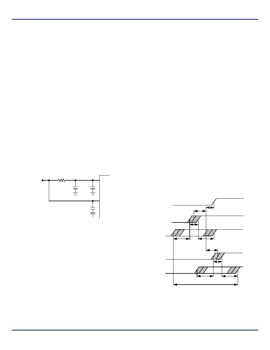
Figure 7. VCC_PLL Power Supply Filter
The minimum values for RF and the filter capacitor CF are
defined by the required filter characteristics: the RC filter
should provide an attenuation greater than 40 dB for noise
whose spectral content is above 100 kHz. In the example RC
filter shown in Figure 7, the filter cut-off frequency is around
4.5 kHz and the noise attenuation at 100 kHz is better than
42 dB.
As the noise frequency crosses the series resonant point
of an individual capacitor its overall impedance begins to look
inductive and thus increases with increasing frequency. The
parallel capacitor combination shown ensures that a low
impedance path to ground exists for frequencies well above
the bandwidth of the PLL. Although the MPC9772 has
several design features to minimize the susceptibility to
power supply noise (isolated power and grounds and fully
differential PLL) there still may be applications in which
overall performance is being degraded due to system power
supply noise. The power supply filter schemes discussed in
this section should be adequate to eliminate power supply
noise related problems in most designs.
Using the MPC9772 in Zero-Delay Applications
Nested clock trees are typical applications for the
MPC9772. Designs using the MPC9772 as LVCMOS PLL
fanout buffer with zero insertion delay will show significantly
lower clock skew than clock distributions developed from
CMOS fanout buffers. The external feedback option of the
MPC9772 clock driver allows for its use as a zero delay
buffer. The PLL aligns the feedback clock output edge with
the clock input reference edge resulting a near zero delay
through the device (the propagation delay through the device
is virtually eliminated). The maximum insertion delay of the
device in zero-delay applications is measured between the
reference clock input and any output. This effective delay
consists of the static phase offset, I/O jitter (phase or
long-term jitter), feedback path delay and the
output-to-output skew error relative to the feedback output.
Calculation of Part-to-Part Skew
The MPC9772 zero delay buffer supports applications
where critical clock signal timing can be maintained across
several devices. If the reference clock inputs of two or more
MPC9772 are connected together, the maximum overall
timing uncertainty from the common CCLKx input to any
output is:
tSK(PP) = t() + tSK(O) + tPD, LINE(FB) + tJIT() CF
This maximum timing uncertainty consist of 4 components:
static phase offset, output skew, feedback board trace delay
and I/O (phase) jitter:
Figure 8. MPC9772 Maximum
Device-to-Device Skew
Due to the statistical nature of I/O jitter a RMS value (1
)
is specified. I/O jitter numbers for other confidence factors
VCC_PLL
VCC
MPC9772
10 nF
RF = 5–10
CF
33...100 nF
RF
VCC
CF = 22 F
tPD,LINE(FB)
tJIT()
+tSK(O)
–t()
+t()
tJIT()
+tSK(O)
tSK(PP)
Max. skew
CCLKCommon
QFBDevice 1
Any QDevice 1
QFBDevice2
Any QDevice 2
相关PDF资料 |
PDF描述 |
|---|---|
| MPC9774FAR2 | IC PLL CLK GEN 1:14 3.3V 52-LQFP |
| MPC97H74AE | IC PLL CLK GEN 1:14 3.3V 52-LQFP |
| MPC9993AC | IC PLL CLK DRIVER IDCS 32-LQFP |
| MPC99J93AC | IC PLL CLK DRIVER IDCS 32-LQFP |
| MPR032EPR2 | IC CTLR TOUCH SENSOR 8-DFN |
相关代理商/技术参数 |
参数描述 |
|---|---|
| MPC9772FAR2 | 功能描述:时钟发生器及支持产品 FSL 1-12 LVCMOS PLL Clock Generator, xta RoHS:否 制造商:Silicon Labs 类型:Clock Generators 最大输入频率:14.318 MHz 最大输出频率:166 MHz 输出端数量:16 占空比 - 最大:55 % 工作电源电压:3.3 V 工作电源电流:1 mA 最大工作温度:+ 85 C 安装风格:SMD/SMT 封装 / 箱体:QFN-56 |
| MPC9773 | 制造商:FREESCALE 制造商全称:Freescale Semiconductor, Inc 功能描述:3.3 V 1:12 LVCMOS PLL Clock Generator |
| MPC9773AE | 功能描述:时钟发生器及支持产品 FSL 1-12 LVCMOS/LVPE CL to LVCMOS PLL Clo RoHS:否 制造商:Silicon Labs 类型:Clock Generators 最大输入频率:14.318 MHz 最大输出频率:166 MHz 输出端数量:16 占空比 - 最大:55 % 工作电源电压:3.3 V 工作电源电流:1 mA 最大工作温度:+ 85 C 安装风格:SMD/SMT 封装 / 箱体:QFN-56 |
| MPC9773AER2 | 功能描述:时钟发生器及支持产品 FSL 1-12 LVCMOS/LVPE CL to LVCMOS PLL Clo RoHS:否 制造商:Silicon Labs 类型:Clock Generators 最大输入频率:14.318 MHz 最大输出频率:166 MHz 输出端数量:16 占空比 - 最大:55 % 工作电源电压:3.3 V 工作电源电流:1 mA 最大工作温度:+ 85 C 安装风格:SMD/SMT 封装 / 箱体:QFN-56 |
| MPC9773FA | 功能描述:锁相环 - PLL 3.3V 240MHz Clock Generator RoHS:否 制造商:Silicon Labs 类型:PLL Clock Multiplier 电路数量:1 最大输入频率:710 MHz 最小输入频率:0.002 MHz 输出频率范围:0.002 MHz to 808 MHz 电源电压-最大:3.63 V 电源电压-最小:1.71 V 最大工作温度:+ 85 C 最小工作温度:- 40 C 封装 / 箱体:QFN-36 封装:Tray |
发布紧急采购,3分钟左右您将得到回复。