- 您现在的位置:买卖IC网 > Datasheet目录344 > MSC8122ADSE (Freescale Semiconductor)KIT ADVANCED DEV SYSTEM 8122 Datasheet资料下载
参数资料
| 型号: | MSC8122ADSE |
| 厂商: | Freescale Semiconductor |
| 文件页数: | 41/48页 |
| 文件大小: | 0K |
| 描述: | KIT ADVANCED DEV SYSTEM 8122 |
| 标准包装: | 1 |
| 系列: | StarCore |
| 类型: | DSP |
| 适用于相关产品: | MSC8122 |
| 所含物品: | 板 |
| 相关产品: | MSC8122TVT6400-ND - DSP 16BIT 400MHZ MULTI 431FCPBGA MSC8122TMP6400V-ND - DSP 16BIT 400MHZ MULTI 431FCPBGA MSC8122TMP6400-ND - DSP 16BIT 400MHZ MULTI 431FCPBGA MSC8122TMP4800V-ND - DSP 16BIT 300MHZ MULTI 431FCPBGA MSC8122MP8000-ND - DSP 16BIT 500MHZ MULTI 431FCPBGA MSC8122VT8000-ND - IC DSP QUAD 16B 500MHZ 431FCPBGA MSC8122TVT6400V-ND - IC DSP QUAD 16B 400MHZ 431FCPBGA MSC8122TVT4800V-ND - IC DSP QUAD 16B 300MHZ 431FCPBGA |
第1页第2页第3页第4页第5页第6页第7页第8页第9页第10页第11页第12页第13页第14页第15页第16页第17页第18页第19页第20页第21页第22页第23页第24页第25页第26页第27页第28页第29页第30页第31页第32页第33页第34页第35页第36页第37页第38页第39页第40页当前第41页第42页第43页第44页第45页第46页第47页第48页
�� �
�
�Hardware� Design� Considerations�
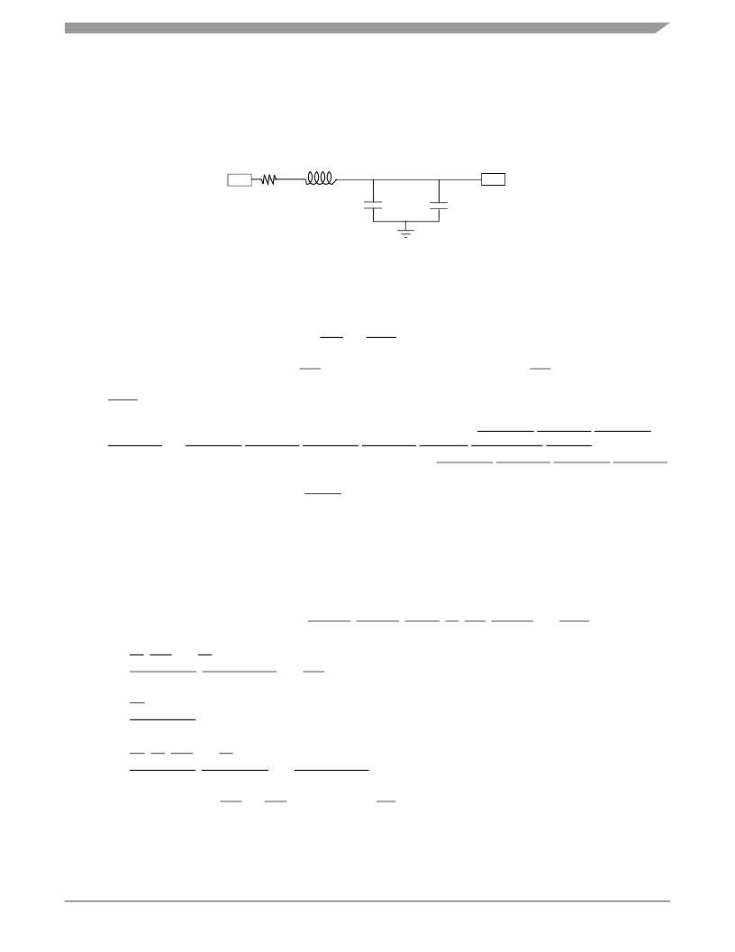
�Figure� 34� .� For� optimal� noise� filtering,� place� the� circuit� as� close� as� possible� to� V� CCSYN� .� The� 0.01-μF� capacitor� should� be� closest�
�to� V� CCSYN� ,� followed� by� the� 10-μF� capacitor,� the� 10-nH� inductor,� and� finally� the� 10-� Ω� resistor� to� V� DD� .� These� traces� should� be�
�kept� short� and� direct.� Provide� an� extremely� low� impedance� path� to� the� ground� plane� for� GND� SYN� .� Bypass� GND� SYN� to� V� CCSYN�
�by� a� 0.01-μF� capacitor� located� as� close� as� possible� to� the� chip� package.� For� best� results,� place� this� capacitor� on� the� backside� of�
�the� PCB� aligned� with� the� depopulated� void� on� the� MSC8122� located� in� the� square� defined� by� positions,� L11,� L12,� L13,� M11,�
�M12,� M13,� N11,� N12,� and� N13.�
�V� DD�
�10� Ω�
�10nH�
�V� CCSYN�
�10� μF�
�Figure� 34.� V� CCSYN� Bypass�
�0.01� μF�
�3.3�
�Connectivity� Guidelines�
�Unused� output� pins� can� be� disconnected,� and� unused� input� pins� should� be� connected� to� the� non-active� value,� via� resistors� to�
�V� DDH� or� GND� ,� except� for� the� following:�
�?�
�?�
�?�
�?�
�?�
�?�
�?�
�?�
�?�
�?�
�?�
�If� the� DSI� is� unused� (DDR[DSIDIS]� is� set),� HCS� and� HBCS� must� pulled� up� and� all� the� rest� of� the� DSI� signals� can� be�
�disconnected.�
�When� the� DSI� uses� synchronous� mode,� HTA� must� be� pulled� up.� In� asynchronous� mode,� HTA� should� be� pulled� either�
�up� or� down,� depending� on� design� requirements.�
�HDST� can� be� disconnected� if� the� DSI� is� in� big-endian� mode,� or� if� the� DSI� is� in� little-endian� mode� and� the�
�DCR[DSRFA]� bit� is� set.�
�When� the� DSI� is� in� 64-bit� data� bus� mode� and� DCR[BEM]� is� cleared,� pull� up� HWBS[1–3]� /� HDBS[1–3]� /� HWBE[1–3]� /�
�HDBE[1–3]� and� HWBS[4–7]� /� HDBS[4–7]� /� HWBE[4–7]� /� HDBE[4–7]� /� PWE[4–7]� /� PSDDQM[4–7]� /� PBS[4–7]� .�
�When� the� DSI� is� in� 32-bit� data� bus� mode� and� DCR[BEM]� is� cleared,� HWBS[1–3]� /� HDBS[1–3]� /� HWBE[1–3]� /� HDBE[1–3]�
�must� be� pulled� up.�
�When� the� DSI� is� in� asynchronous� mode,� HBRST� and� HCLKIN� should� either� be� disconnected� or� pulled� up.�
�When� the� DSI� uses� sliding� window� address� mode� (DCR[SLDWA]� =� 1),� the� external� HA[11–13]� signals� must� be�
�connected� (tied)� to� the� correct� voltage� levels� so� that� the� host� can� perform� the� first� access� to� the� DCR.� After� reset,� the�
�DSI� expects� full� address� mode� (DCR[SLDWA]� =� 0).� The� DCR� address� in� the� DSI� memory� map� is� 0x1BE000,� which�
�requires� the� following� connections:�
�—� HA11� must� be� pulled� high� (1)�
�—� HA12� must� be� pulled� high� (1)�
�—� HA13� must� be� pulled� low� (0)�
�The� following� signals� must� be� pulled� up:� HRESET� ,� SRESET� ,� ARTRY� ,� TA� ,� TEA� ,� PSDVAL� ,� and� AACK� .�
�In� single-master� mode� (BCR[EBM]� =� 0)� with� internal� arbitration� (PPC_ACR[EARB]� =� 0):�
�—� BG� ,� DBG� ,� and� TS� can� be� left� unconnected.�
�—� EXT_BG[2–3]� ,� EXT_DBG[2–3]� ,� and� GBL� can� be� left� unconnected� if� they� are� multiplexed� to� the� system� bus�
�functionality.� For� any� other� functionality,� connect� the� signal� lines� based� on� the� multiplexed� functionality.�
�—� BR� must� be� pulled� up.�
�—� EXT_BR[2–3]� must� be� pulled� up� if� multiplexed� to� the� system� bus� functionality.�
�If� there� is� an� external� bus� master� (BCR[EBM]� =� 1):�
�—� BR� ,� BG� ,� DBG� ,� and� TS� must� be� pulled� up.�
�—� EXT_BR[2–3]� ,� EXT_BG[2–3]� ,� and� EXT_DBG[2–3]� must� be� pulled� up� if� multiplexed� to� the� system� bus�
�functionality.�
�In� single-master� mode,� ABB� and� DBB� can� be� selected� as� IRQ� inputs� and� be� connected� to� the� non-active� value.� In� other�
�modes,� they� must� be� pulled� up.�
�MSC8122� Quad� Digital� Signal� Processor� Data� Sheet,� Rev.� 16�
�Freescale� Semiconductor�
�41�
�相关PDF资料 |
PDF描述 |
|---|---|
| MSC8126ADSE | KIT ADVANCED DEV SYSTEM 8126 |
| MSC8144ADS | ADS FOR MSC8144 DEVICE |
| MSC8156EVM | EVAL MODULE FOR MSC8156 LC |
| MSL1060AW | IC LED DRIVER 6 STRING |
| MSL1061AV | IC LED DRIVER 6 STRING |
相关代理商/技术参数 |
参数描述 |
|---|---|
| MSC8122MP8000 | 功能描述:DSP 16BIT 500MHZ MULTI 431FCPBGA RoHS:否 类别:集成电路 (IC) >> 嵌入式 - DSP(数字式信号处理器) 系列:StarCore 标准包装:40 系列:TMS320DM64x, DaVinci™ 类型:定点 接口:I²C,McASP,McBSP 时钟速率:400MHz 非易失内存:外部 芯片上RAM:160kB 电压 - 输入/输出:3.30V 电压 - 核心:1.20V 工作温度:0°C ~ 90°C 安装类型:表面贴装 封装/外壳:548-BBGA,FCBGA 供应商设备封装:548-FCBGA(27x27) 包装:托盘 配用:TMDSDMK642-0E-ND - DEVELPER KIT W/NTSC CAMERA296-23038-ND - DSP STARTER KIT FOR TMS320C6416296-23059-ND - FLASHBURN PORTING KIT296-23058-ND - EVAL MODULE FOR DM642TMDSDMK642-ND - DEVELOPER KIT W/NTSC CAMERA |
| MSC8122TMP4800V | 功能描述:DSP 16BIT 300MHZ MULTI 431FCPBGA RoHS:否 类别:集成电路 (IC) >> 嵌入式 - DSP(数字式信号处理器) 系列:StarCore 标准包装:40 系列:TMS320DM64x, DaVinci™ 类型:定点 接口:I²C,McASP,McBSP 时钟速率:400MHz 非易失内存:外部 芯片上RAM:160kB 电压 - 输入/输出:3.30V 电压 - 核心:1.20V 工作温度:0°C ~ 90°C 安装类型:表面贴装 封装/外壳:548-BBGA,FCBGA 供应商设备封装:548-FCBGA(27x27) 包装:托盘 配用:TMDSDMK642-0E-ND - DEVELPER KIT W/NTSC CAMERA296-23038-ND - DSP STARTER KIT FOR TMS320C6416296-23059-ND - FLASHBURN PORTING KIT296-23058-ND - EVAL MODULE FOR DM642TMDSDMK642-ND - DEVELOPER KIT W/NTSC CAMERA |
| MSC8122TMP6400 | 功能描述:数字信号处理器和控制器 - DSP, DSC PBGA PB 1.2V 105C 400MHZ RoHS:否 制造商:Microchip Technology 核心:dsPIC 数据总线宽度:16 bit 程序存储器大小:16 KB 数据 RAM 大小:2 KB 最大时钟频率:40 MHz 可编程输入/输出端数量:35 定时器数量:3 设备每秒兆指令数:50 MIPs 工作电源电压:3.3 V 最大工作温度:+ 85 C 封装 / 箱体:TQFP-44 安装风格:SMD/SMT |
| MSC8122TMP6400V | 功能描述:DSP 16BIT 400MHZ MULTI 431FCPBGA RoHS:否 类别:集成电路 (IC) >> 嵌入式 - DSP(数字式信号处理器) 系列:StarCore 标准包装:2 系列:StarCore 类型:SC140 内核 接口:DSI,以太网,RS-232 时钟速率:400MHz 非易失内存:外部 芯片上RAM:1.436MB 电压 - 输入/输出:3.30V 电压 - 核心:1.20V 工作温度:-40°C ~ 105°C 安装类型:表面贴装 封装/外壳:431-BFBGA,FCBGA 供应商设备封装:431-FCPBGA(20x20) 包装:托盘 |
| MSC8122TVT4800V | 功能描述:IC DSP QUAD 16B 300MHZ 431FCPBGA RoHS:是 类别:集成电路 (IC) >> 嵌入式 - DSP(数字式信号处理器) 系列:StarCore 标准包装:2 系列:StarCore 类型:SC140 内核 接口:DSI,以太网,RS-232 时钟速率:400MHz 非易失内存:外部 芯片上RAM:1.436MB 电压 - 输入/输出:3.30V 电压 - 核心:1.20V 工作温度:-40°C ~ 105°C 安装类型:表面贴装 封装/外壳:431-BFBGA,FCBGA 供应商设备封装:431-FCPBGA(20x20) 包装:托盘 |
发布紧急采购,3分钟左右您将得到回复。