- 您现在的位置:买卖IC网 > PDF目录96090 > MTB30N06VL (ON SEMICONDUCTOR) 30 A, 60 V, 0.05 ohm, N-CHANNEL, Si, POWER, MOSFET PDF资料下载
参数资料
| 型号: | MTB30N06VL |
| 厂商: | ON SEMICONDUCTOR |
| 元件分类: | JFETs |
| 英文描述: | 30 A, 60 V, 0.05 ohm, N-CHANNEL, Si, POWER, MOSFET |
| 封装: | CASE 418B-03, D2PAK-3 |
| 文件页数: | 1/10页 |
| 文件大小: | 259K |
| 代理商: | MTB30N06VL |
Semiconductor Components Industries, LLC, 2006
August, 2006 Rev. 6
1
Publication Order Number:
MTB30N06VL/D
MTB30N06VL
Preferred Device
Power MOSFET
30 Amps, 60 Volts, Logic Level
NChannel D2PAK
This Power MOSFET is designed to withstand high energy in the
avalanche and commutation modes. Designed for low voltage, high
speed switching applications in power supplies, converters and power
motor controls, these devices are particularly well suited for bridge
circuits where diode speed and commutating safe operating areas are
critical and offer additional safety margin against unexpected voltage
transients.
Avalanche Energy Specified
IDSS and VDS(on) Specified at Elevated Temperature
MAXIMUM RATINGS (TC = 25°C unless otherwise noted)
Rating
Symbol
Value
Unit
DraintoSource Voltage
VDSS
60
Vdc
DraintoGate Voltage (RGS = 1.0 MΩ)
VDGR
60
Vdc
GatetoSource Voltage
Continuous
NonRepetitive (tp ≤ 10 ms)
VGS
VGSM
± 15
± 20
Vdc
Vpk
Drain Current Continuous
Drain Current Continuous @ 100°C
Drain Current Single Pulse (tp ≤ 10 μs)
ID
IDM
30
20
105
Adc
Apk
Total Power Dissipation
Derate above 25°C
Total Power Dissipation @ TA = 25°C
(Note 1.)
PD
90
0.6
3.0
Watts
W/°C
Watts
Operating and Storage Temperature
Range
TJ, Tstg
55 to
175
°C
Single Pulse DraintoSource Avalanche
Energy Starting TJ = 25°C
(VDD = 25 Vdc, VGS = 5 Vdc, Peak
IL = 30 Apk, L = 0.342 mH, RG = 25 Ω)
EAS
154
mJ
Thermal Resistance
Junction to Case
Junction to Ambient
Junction to Ambient (Note 1.)
RθJC
RθJA
1.67
62.5
50
°C/W
Maximum Lead Temperature for Soldering
Purposes, 1/8″ from Case for 10
seconds
TL
260
°C
1. When surface mounted to an FR4 board using the minimum recommended
pad size.
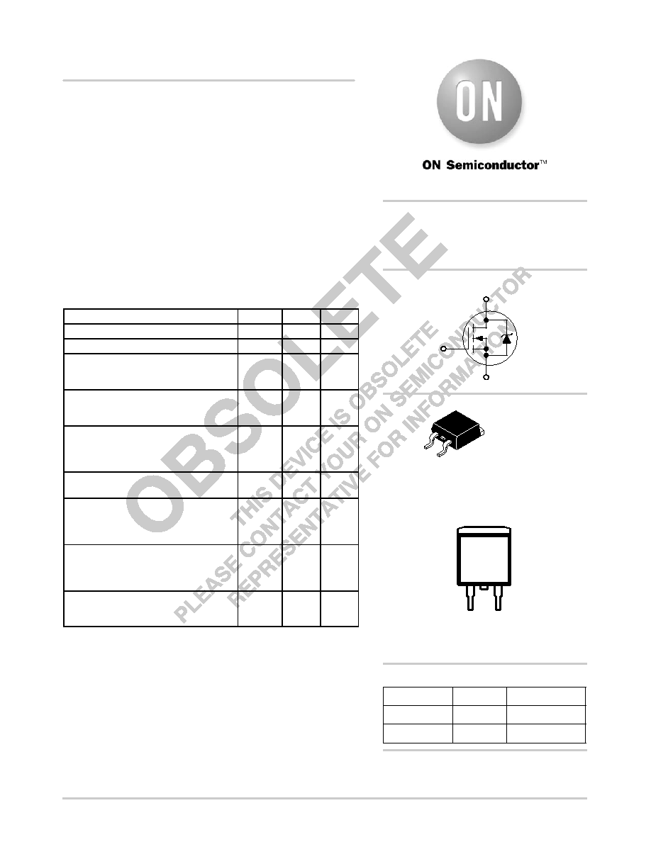
MARKING DIAGRAM
& PIN ASSIGNMENT
T30N06VL
YWW
1
Gate
4
Drain
2
Drain
3
Source
30 AMPERES
60 VOLTS
RDS(on) = 50 mΩ
Device
Package
Shipping
ORDERING INFORMATION
MTB30N06VL
D2PAK
50 Units/Rail
D2PAK
CASE 418B
STYLE 2
1
2
3
4
http://onsemi.com
NChannel
D
S
G
T30N06VL = Device Code
Y
= Year
WW
= Work Week
MTB30N06VLT4
D2PAK
800/Tape & Reel
Preferred devices are recommended choices for future use
and best overall value.
相关PDF资料 |
PDF描述 |
|---|---|
| MTB33N10ET4 | 33 A, 100 V, 0.06 ohm, N-CHANNEL, Si, POWER, MOSFET |
| MTB33N10E | 33 A, 100 V, 0.06 ohm, N-CHANNEL, Si, POWER, MOSFET |
| MTB33N10ET4 | 33 A, 100 V, 0.06 ohm, N-CHANNEL, Si, POWER, MOSFET |
| MTB35N06ZL | 35 A, 60 V, 0.026 ohm, N-CHANNEL, Si, POWER, MOSFET |
| MTB35N06ZLT4 | 35 A, 60 V, 0.026 ohm, N-CHANNEL, Si, POWER, MOSFET |
相关代理商/技术参数 |
参数描述 |
|---|---|
| MTB30N06VLT4 | 制造商:ON Semiconductor 功能描述:Trans MOSFET N-CH 60V 30A 3-Pin(2+Tab) D2PAK T/R |
| MTB30P06 | 制造商:MOTOROLA 制造商全称:Motorola, Inc 功能描述:TMOS POWER FET 30 AMPERES 60 VOLTS |
| MTB30P06V | 制造商:ON Semiconductor 功能描述:Trans MOSFET P-CH 60V 30A 3-Pin(2+Tab) D2PAK Rail |
| MTB30P06VG | 制造商:ON Semiconductor 功能描述:Trans MOSFET P-CH 60V 30A 3-Pin(2+Tab) D2PAK Rail |
| MTB30P06VT4 | 功能描述:MOSFET 60V 30A P-Channel RoHS:否 制造商:STMicroelectronics 晶体管极性:N-Channel 汲极/源极击穿电压:650 V 闸/源击穿电压:25 V 漏极连续电流:130 A 电阻汲极/源极 RDS(导通):0.014 Ohms 配置:Single 最大工作温度: 安装风格:Through Hole 封装 / 箱体:Max247 封装:Tube |
发布紧急采购,3分钟左右您将得到回复。