- 您现在的位置:买卖IC网 > PDF目录96091 > MTD20P03HDL (ON SEMICONDUCTOR) 19 A, 30 V, 0.099 ohm, P-CHANNEL, Si, POWER, MOSFET PDF资料下载
参数资料
| 型号: | MTD20P03HDL |
| 厂商: | ON SEMICONDUCTOR |
| 元件分类: | JFETs |
| 英文描述: | 19 A, 30 V, 0.099 ohm, P-CHANNEL, Si, POWER, MOSFET |
| 封装: | CASE 369C-01, DPAK-3 |
| 文件页数: | 1/9页 |
| 文件大小: | 89K |
| 代理商: | MTD20P03HDL |
Semiconductor Components Industries, LLC, 2006
July, 2006 Rev. 7
1
Publication Order Number:
MTD20P03HDL/D
MTD20P03HDL
Preferred Device
Power MOSFET
20 Amps, 30 Volts, Logic Level
PChannel DPAK
This Power MOSFET is designed to withstand high energy in the
avalanche and commutation modes. This energy efficient design also
offers a draintosource diode with a fast recovery time. Designed for
low voltage, high speed switching applications in power supplies,
converters and PWM motor controls, these devices are particularly
well suited for bridge circuits where diode speed and commutating
safe operating areas are critical and offer additional safety margin
against unexpected voltage transients.
Features
Avalanche Energy Specified
SourcetoDrain Diode Recovery Time Comparable to a Discrete
Fast Recovery Diode
Diode is Characterized for Use in Bridge Circuits
IDSS and VDS(on) Specified at Elevated Temperature
PbFree Packages are Available
MAXIMUM RATINGS (TC = 25°C unless otherwise noted)
Rating
Symbol
Value
Unit
DrainSource Voltage
VDSS
30
Vdc
DrainGate Voltage (RGS = 1.0 MW)
VDGR
30
Vdc
GateSource Voltage
Continuous
NonRepetitive (tpv10 ms)
VGS
VGSM
"15
"20
Vdc
Vpk
Drain Current
Continuous
Continuous @ 100
°C
Single Pulse (tpv10 ms)
ID
IDM
19
12
57
Adc
Apk
Total Power Dissipation
Derate above 25
°C
PD
75
0.6
1.75
W
W/
°C
Operating and Storage Temperature Range
TJ, Tstg
55 to
150
°C
Single Pulse DraintoSource Avalanche
Energy Starting TJ = 25°C
(VDD = 25 Vdc, VGS = 5.0 Vdc,
IL = 19 Apk, L = 1.1 mH, RG = 25 W)
EAS
200
mJ
Thermal Resistance,
JunctiontoCase
JunctiontoAmbient (Note 1)
JunctiontoAmbient (Note 2)
RqJC
RqJA
1.67
100
71.4
°C/W
Maximum Lead Temperature for Soldering
Purposes, 1/8
″ from case for 10 seconds
TL
260
°C
Stresses exceeding Maximum Ratings may damage the device. Maximum
Ratings are stress ratings only. Functional operation above the Recommended
Operating Conditions is not implied. Extended exposure to stresses above the
Recommended Operating Conditions may affect device reliability.
1. When surface mounted to an FR4 board using the minimum recommended
pad size.
2. When surface mounted to an FR4 board using the 0.5 sq.in. drain pad size.
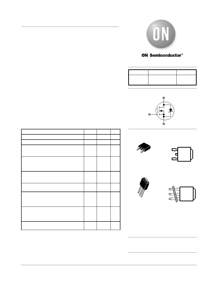
D
S
G
PChannel
Preferred devices are recommended choices for future use
and best overall value.
http://onsemi.com
DPAK
CASE 369C
STYLE 2
MARKING DIAGRAMS
Y
= Year
WW
= Work Week
20P03HL = Device Code
G
= PbFree Package
1 2
3
4
DPAK
CASE 369D
STYLE 2
1
2
3
4
30 V
90 m
W@5.0 V
RDS(on) TYP
20 A
(Note 1)
ID MAX
V(BR)DSS
3 Source
2 Drain
1 Gate
YWW
20P
03HLG
3 Source
2 Drain
1 Gate
YWW
20P
03HLG
See detailed ordering and shipping information in the package
dimensions section on page 7 of this data sheet.
ORDERING INFORMATION
相关PDF资料 |
PDF描述 |
|---|---|
| MTD20P03HDL1 | 19 A, 30 V, 0.099 ohm, P-CHANNEL, Si, POWER, MOSFET |
| MTD20P03HDLT4 | 19 A, 30 V, 0.099 ohm, P-CHANNEL, Si, POWER, MOSFET |
| MTD20P03HDLG | 19 A, 30 V, 0.099 ohm, P-CHANNEL, Si, POWER, MOSFET |
| MTD20P06HDLT4G | 15 A, 60 V, 0.175 ohm, P-CHANNEL, Si, POWER, MOSFET |
| MTD20P06HDLG | 15 A, 60 V, 0.175 ohm, P-CHANNEL, Si, POWER, MOSFET |
相关代理商/技术参数 |
参数描述 |
|---|---|
| MTD20P03HDL1 | 制造商:ON Semiconductor 功能描述:Trans MOSFET P-CH 30V 19A 3-Pin(3+Tab) IPAK Rail 制造商:Rochester Electronics LLC 功能描述:- Bulk |
| MTD20P03HDL1G | 制造商:ON Semiconductor 功能描述:Trans MOSFET P-CH 30V 19A 3-Pin(3+Tab) IPAK Rail |
| MTD20P03HDLT4 | 功能描述:MOSFET P-CH 30V 19A DPAK RoHS:否 类别:分离式半导体产品 >> FET - 单 系列:- 标准包装:1,000 系列:MESH OVERLAY™ FET 型:MOSFET N 通道,金属氧化物 FET 特点:逻辑电平门 漏极至源极电压(Vdss):200V 电流 - 连续漏极(Id) @ 25° C:18A 开态Rds(最大)@ Id, Vgs @ 25° C:180 毫欧 @ 9A,10V Id 时的 Vgs(th)(最大):4V @ 250µA 闸电荷(Qg) @ Vgs:72nC @ 10V 输入电容 (Ciss) @ Vds:1560pF @ 25V 功率 - 最大:40W 安装类型:通孔 封装/外壳:TO-220-3 整包 供应商设备封装:TO-220FP 包装:管件 |
| MTD20P06 | 制造商:MOTOROLA 制造商全称:Motorola, Inc 功能描述:TMOS POWER FET LOGIC LEVEL 15 AMPERES 60 VOLTS RDS(on) = 175 MOHM |
| MTD20P06HDL | 制造商:ON Semiconductor 功能描述:MOSFET P LOGIC D-PAK |
发布紧急采购,3分钟左右您将得到回复。