- 您现在的位置:买卖IC网 > Datasheet目录480 > MTD20P06HDLT4 (ON Semiconductor)MOSFET P-CH 60V 15A DPAK Datasheet资料下载
参数资料
| 型号: | MTD20P06HDLT4 |
| 厂商: | ON Semiconductor |
| 文件页数: | 1/8页 |
| 文件大小: | 0K |
| 描述: | MOSFET P-CH 60V 15A DPAK |
| 产品变化通告: | Product Discontinuation 30/Jun/2004 |
| 标准包装: | 2,500 |
| FET 型: | MOSFET P 通道,金属氧化物 |
| FET 特点: | 逻辑电平门 |
| 漏极至源极电压(Vdss): | 60V |
| 电流 - 连续漏极(Id) @ 25° C: | 15A |
| 开态Rds(最大)@ Id, Vgs @ 25° C: | 175 毫欧 @ 7.5A,5V |
| Id 时的 Vgs(th)(最大): | 2V @ 250µA |
| 闸电荷(Qg) @ Vgs: | 29nC @ 5V |
| 输入电容 (Ciss) @ Vds: | 1190pF @ 25V |
| 功率 - 最大: | 72W |
| 安装类型: | 表面贴装 |
| 封装/外壳: | TO-252-3,DPak(2 引线+接片),SC-63 |
| 供应商设备封装: | DPAK-3 |
| 包装: | 带卷 (TR) |
| 其它名称: | MTD20P06HDLT4OS |
�� �
�
�MTD20P06HDL�
�Preferred� Device�
�Power� MOSFET�
�20� Amps,� 60� Volts,� Logic�
�Level�
�P?Channel� DPAK�
�This� Power� MOSFET� is� designed� to� withstand� high� energy� in� the�
�avalanche� and� commutation� modes.� The� energy� efficient� design� also�
�offers� a� drain?to?source� diode� with� a� fast� recovery� time.� Designed� for�
�low?voltage,� high?speed� switching� applications� in� power� supplies,�
�converters� and� PWM� motor� controls,� and� other� inductive� loads.� The�
�avalanche� energy� capability� is� specified� to� eliminate� the� guesswork� in�
�designs� where� inductive� loads� are� switched,� and� to� offer� additional�
�safety� margin� against� unexpected� voltage� transients.�
�http://onsemi.com�
�20� AMPERES,� 60� VOLTS�
�R� DS(on)� =� 175� m� W�
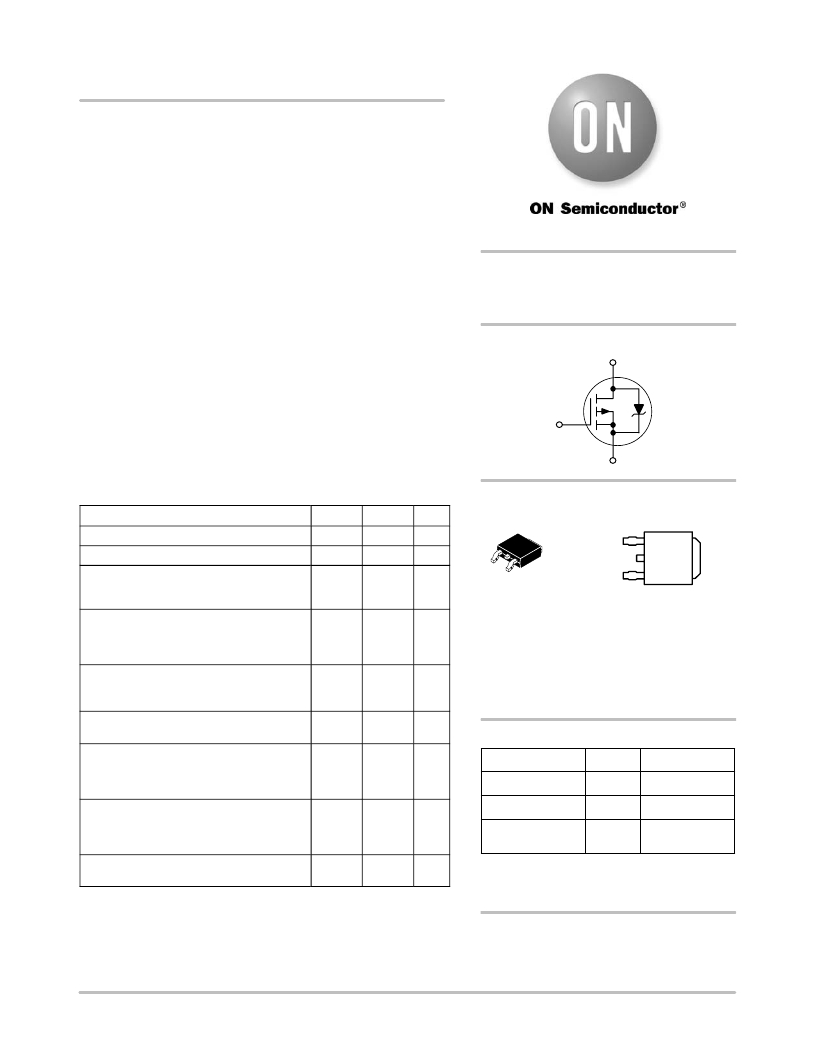
�P?Channel�
�D�
�Features�
�?� Ultra� Low� R� DS(on)� ,� High?Cell� Density,� HDTMOS�
�?� Diode� is� Characterized� for� Use� in� Bridge� Circuits�
�?� I� DSS� and� V� DS(on)� Specified� at� Elevated� Temperature�
�?� Avalanche� Energy� Specified�
�?� Pb?Free� Package� is� Available�
�G�
�S�
�MAXIMUM� RATINGS� (T� C� =� 25� °� C� unless� otherwise� noted)�
�MARKING� DIAGRAM� &� PIN� ASSIGNMENTS�
�Rating�
�Symbol�
�Value�
�Unit�
�Drain?Source� Voltage�
�Drain?Gate� Voltage� (R� GS� =� 1.0� M� W� )�
�Gate?Source� Voltage�
�?� Continuous�
�?� Non?Repetitive� (t� p� v� 10� ms)�
�V� DSS�
�V� DGR�
�V� GS�
�V� GSM�
�60�
�60�
�"� 15�
�"� 20�
�Vdc�
�Vdc�
�Vdc�
�Vpk�
�1� 2�
�3�
�4�
�DPAK�
�CASE� 369C�
�Gate� 1�
�Drain� 2�
�Source� 3�
�YWW�
�20P�
�06HLG�
�4�
�Drain�
�Drain� Current�
�?� Continuous�
�?� Continuous� @� 100� °� C�
�?� Single� Pulse� (t� p� v� 10� m� s)�
�I� D�
�I� D�
�I� DM�
�15�
�9.0�
�45�
�Adc�
�Apk�
�(Surface� Mount)�
�STYLE� 2�
�20P06HL� =� Device� Code�
�Total� Power� Dissipation�
�Derate� above� 25� °� C�
�Total� Power� Dissipation� @� T� C� =� 25� °� C� (Note� 2)�
�Operating� and� Storage� Temperature� Range�
�P� D�
�T� J� ,� T� stg�
�72�
�0.58�
�1.75�
�?55� to�
�W�
�W/� °� C�
�W�
�°� C�
�Y�
�WW�
�G�
�=� Year�
�=� Work� Week�
�=� Pb?Free� Package�
�150�
�ORDERING� INFORMATION�
�Single� Pulse� Drain?to?Source� Avalanche�
�Energy� ?� Starting� T� J� =� 25� °� C�
�E� AS�
�300�
�mJ�
�Device�
�Package�
�Shipping� ?�
�(V� DD� =� 25� Vdc,� V� GS� =� 5.0� Vdc,�
�I� L� =� 15� Apk,� L� =� 2.7� mH,� R� G� =� 25� W� )�
�MTD20P06HDL�
�DPAK�
�75� Units/Rail�
�Thermal� Resistance�
�°� C/W�
�MTD20P06HDLT4�
�DPAK�
�2500� Tape� &� Reel�
�?� Junction?to?Case�
�?� Junction?to?Ambient� (Note� 1)�
�?� Junction?to?Ambient� (Note� 2)�
�R� q� JC�
�R� q� JA�
�R� q� JA�
�1.73�
�100�
�71.4�
�MTD20P06HDLT4G�
�DPAK�
�(Pb?Free)�
�2500� Tape� &� Reel�
�Maximum� Lead� Temperature� for� Soldering� T� L� 260� °� C�
�Purposes,� 1/8� ″� from� case� for� 10� seconds�
�Stresses� exceeding� Maximum� Ratings� may� damage� the� device.� Maximum�
�Ratings� are� stress� ratings� only.� Functional� operation� above� the� Recommended�
�Operating� Conditions� is� not� implied.� Extended� exposure� to� stresses� above� the�
�Recommended� Operating� Conditions� may� affect� device� reliability.�
�1.� When� surface� mounted� to� an� FR4� board� using� the� minimum� recommended�
�pad� size.�
�2.� When� surface� mounted� to� an� FR4� board� using� 0.5� sq.� inch� pad� size.�
�?For� information� on� tape� and� reel� specifications,�
�including� part� orientation� and� tape� sizes,� please�
�refer� to� our� Tape� and� Reel� Packaging� Specification�
�Brochure,� BRD8011/D.�
�Preferred� devices� are� recommended� choices� for� future� use�
�and� best� overall� value.�
�?� Semiconductor� Components� Industries,� LLC,� 2006�
�June,� 2006� ?� Rev.� 6�
�1�
�Publication� Order� Number:�
�MTD20P06HDL/D�
�相关PDF资料 |
PDF描述 |
|---|---|
| MTD2955VT4 | MOSFET P-CH 60V 12A DPAK |
| MTD3010N | PHOTO DIODE 900NM DOME CLR TO-18 |
| MTD3010PM | PHOTO DIODE 900NM DOME CLR TO-18 |
| MTD3055VL | MOSFET N-CH 60V 12A DPAK |
| MTD3055V | MOSFET N-CH 60V 12A DPAK |
相关代理商/技术参数 |
参数描述 |
|---|---|
| MTD214 | 制造商:未知厂家 制造商全称:未知厂家 功能描述:Ethernet Encoder/Decoder and 10BaseT Transceiver with Built-in Waveform Shaper |
| MTD2525J | 制造商:SHINDENGEN 制造商全称:Shindengen Electric Mfg.Co.Ltd 功能描述:DMOS Microstepping Dual PWM Motor Driver |
| MTD2955E | 制造商:MOTOROLA 制造商全称:Motorola, Inc 功能描述:TMOS POWER FET 12 AMPERES 60 VOLTS RDS(on) = 0.3 OHM |
| MTD2955ET4 | 制造商:Motorola Inc 功能描述: |
| MTD2955V | 功能描述:MOSFET DISC BY MFG 2/02 RoHS:否 制造商:STMicroelectronics 晶体管极性:N-Channel 汲极/源极击穿电压:650 V 闸/源击穿电压:25 V 漏极连续电流:130 A 电阻汲极/源极 RDS(导通):0.014 Ohms 配置:Single 最大工作温度: 安装风格:Through Hole 封装 / 箱体:Max247 封装:Tube |
发布紧急采购,3分钟左右您将得到回复。