- 您现在的位置:买卖IC网 > PDF目录97629 > MTP60N06HD (ON SEMICONDUCTOR) 60 A, 60 V, 0.014 ohm, N-CHANNEL, Si, POWER, MOSFET, TO-220AB PDF资料下载
参数资料
| 型号: | MTP60N06HD |
| 厂商: | ON SEMICONDUCTOR |
| 元件分类: | JFETs |
| 英文描述: | 60 A, 60 V, 0.014 ohm, N-CHANNEL, Si, POWER, MOSFET, TO-220AB |
| 封装: | CASE 221A-09, 3 PIN |
| 文件页数: | 6/8页 |
| 文件大小: | 223K |
| 代理商: | MTP60N06HD |
MTP60N06HD
http://onsemi.com
6
I S
,SOURCE
CURRENT
t, TIME
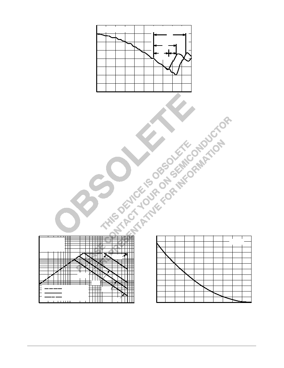
Figure 11. Reverse Recovery Time (trr)
di/dt = 300 A/
μs
Standard Cell Density
High Cell Density
tb
trr
ta
trr
SAFE OPERATING AREA
The Forward Biased Safe Operating Area curves define
the maximum simultaneous draintosource voltage and
drain current that a transistor can handle safely when it is
forward biased. Curves are based upon maximum peak
junction temperature and a case temperature (TC) of 25°C.
Peak repetitive pulsed power limits are determined by using
the thermal response data in conjunction with the procedures
discussed in AN569, “Transient Thermal Resistance
General Data and Its Use.”
Switching between the offstate and the onstate may
traverse any load line provided neither rated peak current
(IDM) nor rated voltage (VDSS) is exceeded, and that the
transition time (tr, tf) does not exceed 10 μs. In addition the
total power averaged over a complete switching cycle must
not exceed (TJ(MAX) TC)/(RθJC).
A power MOSFET designated EFET can be safely used
in switching circuits with unclamped inductive loads. For
reliable operation, the stored energy from circuit inductance
dissipated in the transistor while in avalanche must be less
than the rated limit and must be adjusted for operating
conditions differing from those specified. Although industry
practice is to rate in terms of energy, avalanche energy
capability is not a constant. The energy rating decreases
nonlinearly with an increase of peak current in avalanche
and peak junction temperature.
Although many EFETs can withstand the stress of
draintosource avalanche at currents up to rated pulsed
current (IDM), the energy rating is specified at rated
continuous current (ID), in accordance with industry
custom. The energy rating must be derated for temperature
as shown in the accompanying graph (Figure 13). Maximum
energy at currents below rated continuous ID can safely be
assumed to equal the values indicated.
VDS, DRAINTOSOURCE VOLTAGE (VOLTS)
TJ, STARTING JUNCTION TEMPERATURE (°C)
E
AS
,SINGLE
PULSE
DRAINT
OSOURCE
A
V
ALANCHE
ENERGY
(mJ)
I D
,DRAIN
CURRENT
(AMPS)
Figure 12. Maximum Rated Forward Biased
Safe Operating Area
25
150
50
100
125
75
0
600
400
300
200
100
500
Figure 13. Maximum Avalanche Energy versus
Starting Junction Temperature
0.1
1.0
10
100
1
10
100
1000
dc
100
μs
1 ms
10 ms
10
μs
RDS(on) LIMIT
THERMAL LIMIT
PACKAGE LIMIT
VGS = 20 V
SINGLE PULSE
TC = 25°C
ID = 60 A
相关PDF资料 |
PDF描述 |
|---|---|
| MTP6N60E | 6 A, 600 V, 1.2 ohm, N-CHANNEL, Si, POWER, MOSFET, TO-220AB |
| MTP6N60 | 6 A, 600 V, 1.2 ohm, N-CHANNEL, Si, POWER, MOSFET, TO-220AB |
| MTP6N55 | 6 A, 550 V, 1.2 ohm, N-CHANNEL, Si, POWER, MOSFET, TO-220AB |
| MTP8N10E | 8 A, 100 V, 0.5 ohm, N-CHANNEL, Si, POWER, MOSFET, TO-220AB |
| MTP8N15L | 8 A, 150 V, 0.45 ohm, N-CHANNEL, Si, POWER, MOSFET, TO-220AB |
相关代理商/技术参数 |
参数描述 |
|---|---|
| MTP60N06HD_L86Z | 功能描述:MOSFET DISC BY MFG 2/02 RoHS:否 制造商:STMicroelectronics 晶体管极性:N-Channel 汲极/源极击穿电压:650 V 闸/源击穿电压:25 V 漏极连续电流:130 A 电阻汲极/源极 RDS(导通):0.014 Ohms 配置:Single 最大工作温度: 安装风格:Through Hole 封装 / 箱体:Max247 封装:Tube |
| MTP60N10E7L | 制造商:ON Semiconductor 功能描述: |
| MTP610G | 制造商:ADAM-TECH 制造商全称:Adam Technologies, Inc. 功能描述:MODULAR TELEPHONE PLUGS |
| MTP610U | 制造商:ADAM-TECH 制造商全称:Adam Technologies, Inc. 功能描述:MODULAR TELEPHONE PLUGS |
| MTP610W | 制造商:ADAM-TECH 制造商全称:Adam Technologies, Inc. 功能描述:MODULAR TELEPHONE PLUGS |
发布紧急采购,3分钟左右您将得到回复。