- 您现在的位置:买卖IC网 > PDF目录96108 > MTW35N15E (ON SEMICONDUCTOR) 35 A, 150 V, 0.05 ohm, N-CHANNEL, Si, POWER, MOSFET, TO-247AE PDF资料下载
参数资料
| 型号: | MTW35N15E |
| 厂商: | ON SEMICONDUCTOR |
| 元件分类: | JFETs |
| 英文描述: | 35 A, 150 V, 0.05 ohm, N-CHANNEL, Si, POWER, MOSFET, TO-247AE |
| 封装: | CASE 340K-01, 3 PIN |
| 文件页数: | 1/8页 |
| 文件大小: | 164K |
| 代理商: | MTW35N15E |
Semiconductor Components Industries, LLC, 2005
February, 2005 Rev. XXX
1
Publication Order Number:
MTW35N15E/D
MTW35N15E
Preferred Device
Power MOSFET
35 Amps, 150 Volts
NChannel TO247
This advanced Power MOSFET is designed to withstand high
energy in the avalanche and commutation modes. The new energy
efficient design also offers a draintosource diode with a fast
recovery time. Designed for low voltage, high speed switching
applications in power supplies, converters and PWM motor controls,
these devices are particularly well suited for bridge circuits where
diode speed and commutating safe operating areas are critical and
offer additional safety margin against unexpected voltage transients.
Avalanche Energy Specified
SourcetoDrain Diode Recovery Time Comparable to a Discrete
Fast Recovery Diode
Diode is Characterized for Use in Bridge Circuits
I
DSS and VDS(on) Specified at Elevated Temperature
Isolated Mounting Hole Reduces Mounting Hardware
MAXIMUM RATINGS (TC = 25°C unless otherwise noted)
Rating
Symbol
Value
Unit
DrainSource Voltage
VDSS
150
Vdc
DrainGate Voltage (RGS = 1.0 M)
VDGR
150
Vdc
GateSource Voltage
Continuous
NonRepetitive (tp ≤ 10 ms)
VGS
VGSM
± 20
± 40
Vdc
Vpk
Drain Current Continuous
Drain Current Continuous @ 100
°C
Drain Current Single Pulse (tp ≤ 10 s)
ID
IDM
35
26.9
105
Adc
Apk
Total Power Dissipation
Derate above 25
°C
PD
180
1.45
Watts
W/
°C
Operating and Storage Temperature Range
TJ, Tstg
55 to
150
°C
Single Pulse DraintoSource Avalanche
Energy Starting TJ = 25°C
(VDD = 80 Vdc, VGS = 10 Vdc,
IL = 20 Apk, L = 3.0 mH, RG = 25 )
EAS
600
mJ
Thermal Resistance Junction to Case
Thermal Resistance Junction to Ambient
RθJC
RθJA
0.70
62.5
°C/W
Maximum Lead Temperature for Soldering
Purposes, 1/8
″ from case for 10 seconds
TL
260
°C
Device
Package
Shipping
ORDERING INFORMATION
MTW35N15E
TO247
30 Units/Rail
Preferred devices are recommended choices for future use
and best overall value.
LL
= Location Code
Y
= Year
WW
= Work Week
MTW35N15E
LLYWW
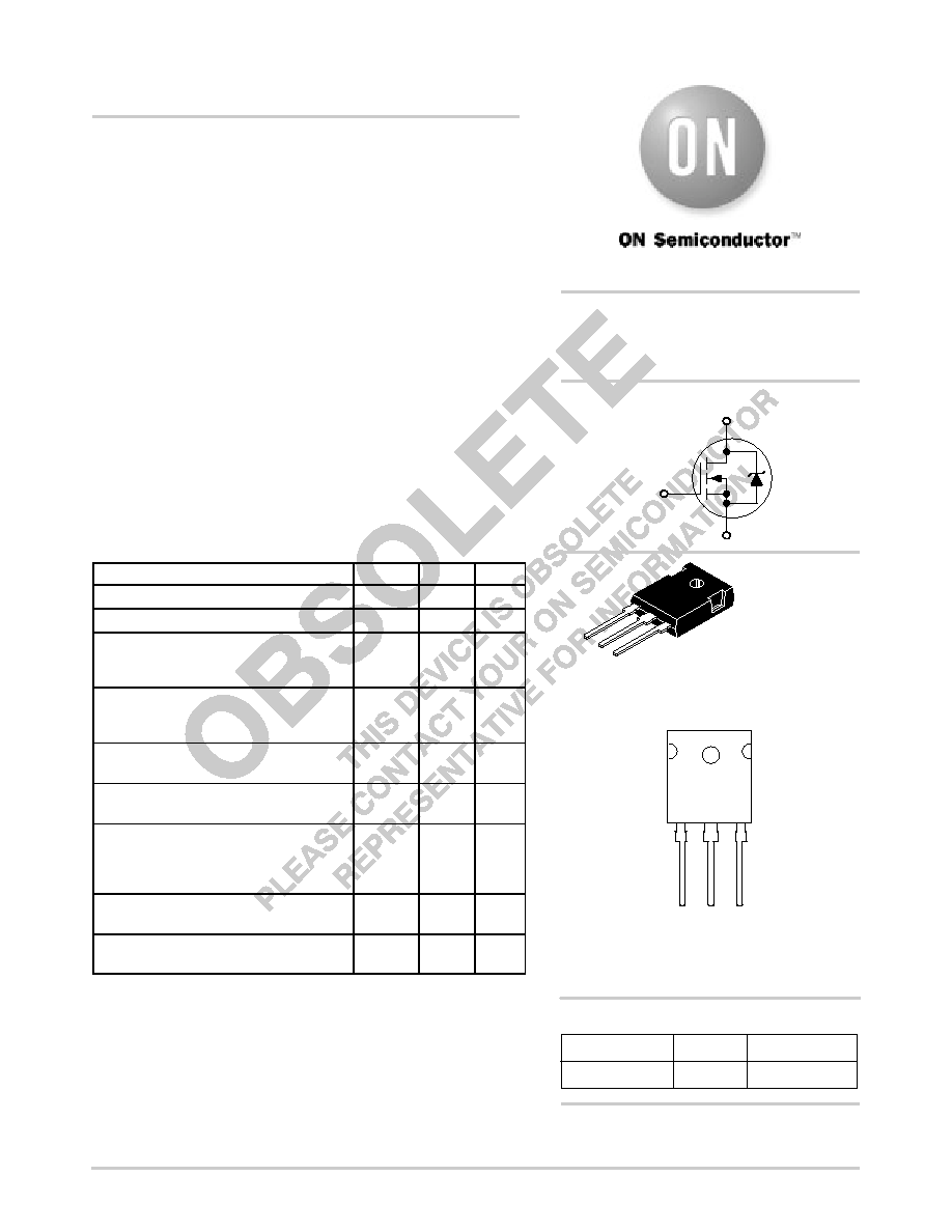
http://onsemi.com
MARKING DIAGRAM
& PIN ASSIGNMENT
D
G
TO247AE
CASE 340K
Style 1
NChannel
S
35 AMPERES
150 VOLTS
RDS(on) = 50 m
1
2
3
4
1
Gate
3
Source
4
Drain
2
Drain
相关PDF资料 |
PDF描述 |
|---|---|
| MTW45N10E | 45 A, 100 V, 0.035 ohm, N-CHANNEL, Si, POWER, MOSFET, TO-247AE |
| MTW7N80E | 7 A, 800 V, 1 ohm, N-CHANNEL, Si, POWER, MOSFET, TO-247AE |
| MTY100N10E | 100 A, 100 V, 0.011 ohm, N-CHANNEL, Si, POWER, MOSFET, TO-264AA |
| MTZJ33B | 33 V, 0.5 W, SILICON, UNIDIRECTIONAL VOLTAGE REGULATOR DIODE, DO-34 |
| MTZJ36B | 36 V, 0.5 W, SILICON, UNIDIRECTIONAL VOLTAGE REGULATOR DIODE, DO-34 |
相关代理商/技术参数 |
参数描述 |
|---|---|
| MTW45N10 | 制造商:MOTOROLA 制造商全称:Motorola, Inc 功能描述:TMOS POWER FET 45 AMPERES 100 VOLTS RDS(on) = 0.035 OHM |
| MTW45N10E | 制造商:Rochester Electronics LLC 功能描述: |
| MTW4N80 | 制造商:MOTOROLA 制造商全称:Motorola, Inc 功能描述:TMOS E-FET POWER FIELD EFFECT TRANSISITOR N-CHANNEL ENHANCEMENT-MODE SILICON GATE |
| MTW4N80E | 制造商:MOTOROLA 制造商全称:Motorola, Inc 功能描述:TMOS E-FET POWER FIELD EFFECT TRANSISITOR N-CHANNEL ENHANCEMENT-MODE SILICON GATE |
| MTW54N05E | 制造商:MOTOROLA 制造商全称:Motorola, Inc 功能描述:High Energy in the Avalanche and Commutation modes |
发布紧急采购,3分钟左右您将得到回复。