- 您现在的位置:买卖IC网 > PDF目录96108 > MTW35N15E (ON SEMICONDUCTOR) 35 A, 150 V, 0.05 ohm, N-CHANNEL, Si, POWER, MOSFET, TO-247AE PDF资料下载
参数资料
| 型号: | MTW35N15E |
| 厂商: | ON SEMICONDUCTOR |
| 元件分类: | JFETs |
| 英文描述: | 35 A, 150 V, 0.05 ohm, N-CHANNEL, Si, POWER, MOSFET, TO-247AE |
| 封装: | CASE 340K-01, 3 PIN |
| 文件页数: | 5/8页 |
| 文件大小: | 164K |
| 代理商: | MTW35N15E |
MTW35N15E
http://onsemi.com
5
DRAINTOSOURCE DIODE CHARACTERISTICS
0.5
0.6
0.7
0.8
0.95
0
5
15
25
35
VSD, SOURCETODRAIN VOLTAGE (VOLTS)
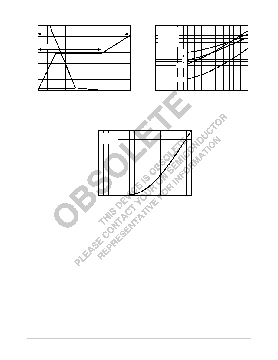
Figure 8. GateToSource and DrainToSource
Voltage versus Total Charge
I S
,SOURCE
CURRENT
(AMPS)
Figure 9. Resistive Switching Time
Variation versus Gate Resistance
RG, GATE RESISTANCE (OHMS)
0
10
100
1000
100
10
t,TIME
(ns)
VDD = 75 V
ID = 35 A
VGS = 10 V
TJ = 25°C
tr
tf
td(off)
td(on)
VGS = 0 V
TJ = 25°C
Figure 10. Diode Forward Voltage versus Current
120
V GS
,GA
TET
OSOURCE
VOL
TAGE
(VOL
TS)
100
60
40
20
0
8.0
4.0
0
QT, TOTAL CHARGE (nC)
VDS
,DRAINT
OSOURCE
VOL
TAGE
(VOL
TS)
12
6.0
2.0
20
80
100
VGS
40
0.55
0.65
0.75
0.85
10
20
30
VDS
Q2
Q1
Q3
60
10
80
QT
TJ = 25°C
ID = 35 A
0.9
SAFE OPERATING AREA
The Forward Biased Safe Operating Area curves define
the maximum simultaneous draintosource voltage and
drain current that a transistor can handle safely when it is
forward biased. Curves are based upon maximum peak
junction temperature and a case temperature (TC) of 25°C.
Peak repetitive pulsed power limits are determined by using
the thermal response data in conjunction with the procedures
discussed
in
AN569,
“Transient
Thermal
ResistanceGeneral Data and Its Use.”
Switching between the offstate and the onstate may
traverse any load line provided neither rated peak current
(IDM) nor rated voltage (VDSS) is exceeded and the
transition time (tr,tf) do not exceed 10 s. In addition the total
power averaged over a complete switching cycle must not
exceed (TJ(MAX) TC)/(RθJC).
A Power MOSFET designated EFET can be safely used
in switching circuits with unclamped inductive loads. For
reliable operation, the stored energy from circuit inductance
dissipated in the transistor while in avalanche must be less
than the rated limit and adjusted for operating conditions
differing from those specified. Although industry practice is
to rate in terms of energy, avalanche energy capability is not
a constant. The energy rating decreases nonlinearly with an
increase of peak current in avalanche and peak junction
temperature.
Although many EFETs can withstand the stress of
draintosource avalanche at currents up to rated pulsed
current (IDM), the energy rating is specified at rated
continuous current (ID), in accordance with industry
custom. The energy rating must be derated for temperature
as shown in the accompanying graph (Figure 12). Maximum
energy at currents below rated continuous ID can safely be
assumed to equal the values indicated.
相关PDF资料 |
PDF描述 |
|---|---|
| MTW45N10E | 45 A, 100 V, 0.035 ohm, N-CHANNEL, Si, POWER, MOSFET, TO-247AE |
| MTW7N80E | 7 A, 800 V, 1 ohm, N-CHANNEL, Si, POWER, MOSFET, TO-247AE |
| MTY100N10E | 100 A, 100 V, 0.011 ohm, N-CHANNEL, Si, POWER, MOSFET, TO-264AA |
| MTZJ33B | 33 V, 0.5 W, SILICON, UNIDIRECTIONAL VOLTAGE REGULATOR DIODE, DO-34 |
| MTZJ36B | 36 V, 0.5 W, SILICON, UNIDIRECTIONAL VOLTAGE REGULATOR DIODE, DO-34 |
相关代理商/技术参数 |
参数描述 |
|---|---|
| MTW45N10 | 制造商:MOTOROLA 制造商全称:Motorola, Inc 功能描述:TMOS POWER FET 45 AMPERES 100 VOLTS RDS(on) = 0.035 OHM |
| MTW45N10E | 制造商:Rochester Electronics LLC 功能描述: |
| MTW4N80 | 制造商:MOTOROLA 制造商全称:Motorola, Inc 功能描述:TMOS E-FET POWER FIELD EFFECT TRANSISITOR N-CHANNEL ENHANCEMENT-MODE SILICON GATE |
| MTW4N80E | 制造商:MOTOROLA 制造商全称:Motorola, Inc 功能描述:TMOS E-FET POWER FIELD EFFECT TRANSISITOR N-CHANNEL ENHANCEMENT-MODE SILICON GATE |
| MTW54N05E | 制造商:MOTOROLA 制造商全称:Motorola, Inc 功能描述:High Energy in the Avalanche and Commutation modes |
发布紧急采购,3分钟左右您将得到回复。