- 您现在的位置:买卖IC网 > PDF目录11791 > NCN6001DTBR2G (ON Semiconductor)IC INTERFACE SMART CARD 20TSSOP PDF资料下载
参数资料
| 型号: | NCN6001DTBR2G |
| 厂商: | ON Semiconductor |
| 文件页数: | 32/36页 |
| 文件大小: | 0K |
| 描述: | IC INTERFACE SMART CARD 20TSSOP |
| 标准包装: | 1 |
| 应用: | 智能卡 |
| 接口: | 微控制器 |
| 电源电压: | 2.75 V ~ 5.5 V |
| 封装/外壳: | 20-TSSOP(0.173",4.40mm 宽) |
| 供应商设备封装: | 20-TSSOP |
| 包装: | 标准包装 |
| 安装类型: | 表面贴装 |
| 其它名称: | NCN6001DTBR2GOSDKR |
第1页第2页第3页第4页第5页第6页第7页第8页第9页第10页第11页第12页第13页第14页第15页第16页第17页第18页第19页第20页第21页第22页第23页第24页第25页第26页第27页第28页第29页第30页第31页当前第32页第33页第34页第35页第36页
NCN6001
http://onsemi.com
5
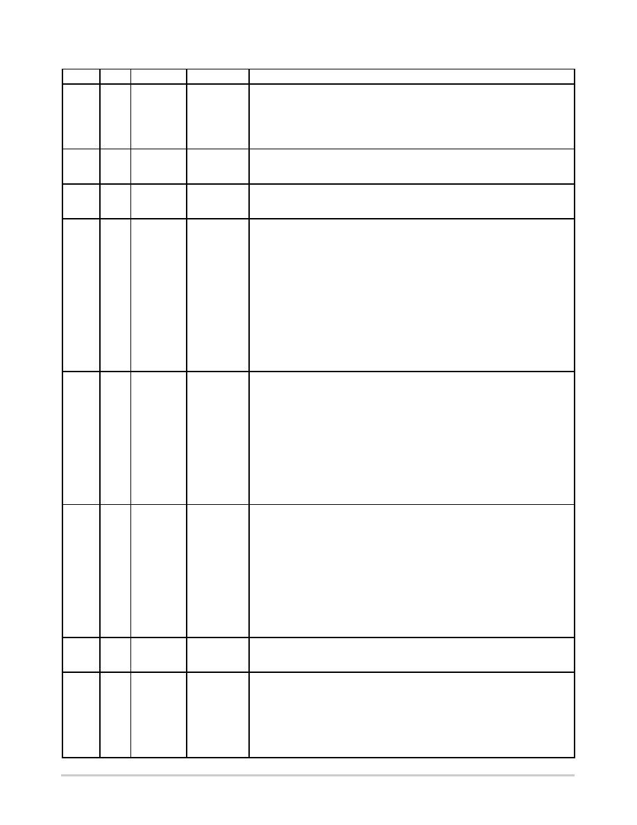
PIN FUNCTIONS AND DESCRIPTION
TSSOP
Description
Type
Name
LLGA
10
7
Lout_L
POWER
The Low Side of the external inductor is connected between this pin and pin 12 to
provide the DC/DC function. The current flowing into this inductor is internally sensed
and no external shunt resistor is used. Typically, Lout = 22 mH, with DSR < 2.0 W,
yields a good efficiency performance for a maximum 65 mA DC output load.
Note: The inductor shall be sized to handle the 450 mA peak current flowing during
the DC/DC operation (see CoilCraft manufacturer data sheet).
11
8
PWR_GND
POWER
This pin is the Power Ground associated with the builtin DC/DC converter and must
be connected to the system ground together with GROUND pin 16. Using good quality
ground plane is recommended to avoid spikes on the logic signal lines.
12
9
Lout_H
POWER
The High Side of the external inductor is connected between this pin and pin 10 to
activate the DC/DC function. The builtin NMOS and PMOS devices provide the
switching function together with the CRD_VCC voltage rectification (Figure 17).
13
10
CRD_VCC
POWER
This pin provides the power to the external card. It is the logic level “1” for CRD_IO,
CRD_RST, CRD_C4, CRD_C8 and CRD_CLK signals.
The energy stored by the DC/DC external inductor Lout must be smoothed by a
10 mF/Low ESR capacitor, connected across CRD_VCC and GND. Using ceramic
type of capacitor (MURATA X5R, ESR < 50 mW) is strongly recommended. In the
event of a CRD_VCC UVLOW voltage, the NCN6001 detects the situation and
feedback the information in the STATUS bit. The device does not take any further
action, particularly the DC/DC converter is neither stopped nor re programmed by the
NCN6001. It is up to the external MPU to handle the situation.
However, when the CRD_VCC is overloaded, the NCN6001 shuts off the DC/DC
converter, runs a Power Down ISO sequence and reports the fault in the STATUS
register.
Since high transient current flows from this pin to the load, care must be observed, at
PCB level, to minimize the series ESR and ESL parasitic values. The NCN6001 demo
board provides an example of a preferred PCB layout.
14
11
C8/S1
I/O
Auxiliary mixed analog/digital line to handle either a synchronous card, or as Chip
Select Identification (MISO, Bit 0): see Figure 9. The pin is driven by an open drain
stage, the pullup resistor being connected to the CRD_VCC supply. When the pin is
used as a logic input (asynchronous cards), the positive logic condition applies:
Connected to GND Logic = Zero
Connected to VCC or left Open Logic = One
A builtin accelerator circuit makes sure the output positive going rise time is fully
within the ISO/EMV specifications.
NOTE: The pin is capable of reading the logic level when the chip operates an
asynchronous interface, but is not intended to read the data from the
external card when operated in the synchronous mode. It merely returns the
logic state forced during a write instruction to the card.
15
12
C4/S0
I/O
Auxiliary mixed analog/digital line to handle either a synchronous card, or as Chip
Select Identification (MISO, Bit 1): see Figure 9. The pin is driven by an open drain
stage, the pullup resistor being connected to the CRD_VCC supply. When the pin is
used as a logic input (asynchronous cards), the positive logic condition applies:
Connected to GND Logic = Zero
Connected to VCC or left Open Logic = One
A builtin accelerator circuit makes sure the output positive going rise time is fully
within the ISO/EMV specifications.
NOTE: The pin is capable of reading the logic level when the chip operates an
asynchronous interface, but is not intended to read the data from the
external card when operated in the synchronous mode. It merely returns the
logic state forced during a write instruction to the card.
16
13
GND
SIGNAL
The logic and low level analog signals shall be connected to this ground pin. This pin
must be externally connected to the PWR_GND pin 12. The designer must make sure
no high current transients are shared with the low signal currents flowing into this pin.
17
14
CRD_CLK
OUTPUT
This pin is connected to the CLK pin of the card connector. The CRD_CLK signal
comes from the clock selector circuit output. An internal active pull down NMOS device
forces this pin to Ground during either the CRD_VCC startup sequence, or when
CRD_VCC = 0 V.
The rise and fall slopes, either FAST or SLOW, of this signal can be programmed by
the MOSI message (Table 2).
Care must be observed, at PCB level, to minimize the pickup noise coming from the
CRD_CLK line.
相关PDF资料 |
PDF描述 |
|---|---|
| AT91SAM7X256B-AU-999 | IC MCU ARM 256KB FLASH 100LQFP |
| ISL36111DRZ-T7 | IC EQUALIZER REC 11.1GBPS 16QFN |
| IA188ES-PQF100I-R-03 | IC MCU 8/16BIT 40MHZ 100PQFP |
| IA186ES-PQF100I-R-03 | IC MCU 8/16BIT 40MHZ 100PQFP |
| QLX4270RIQT7 | IC EQUALIZER REC 2.7GBPS 46QFN |
相关代理商/技术参数 |
参数描述 |
|---|---|
| NCN6001MUTWG | 制造商:ON Semiconductor 功能描述:ANA COMPACT SMARTCARD IC - Tape and Reel 制造商:ON Semiconductor 功能描述:IC INTERFACE SMART CARD 制造商:ON Semiconductor 功能描述:REEL - ANA COMPACT SMARTCARD IC |
| NCN6004A | 制造商:ONSEMI 制造商全称:ON Semiconductor 功能描述:Dual SAM/SIM Interface Integrated Circuit |
| NCN6004A/D | 制造商:ONSEMI 制造商全称:ON Semiconductor 功能描述:Dual SAM/SIM Interface Integrated Circuit |
| NCN6004A_06 | 制造商:ONSEMI 制造商全称:ON Semiconductor 功能描述:Dual SAM/SIM Interface Integrated Circuit |
| NCN6004AFTBR2 | 功能描述:输入/输出控制器接口集成电路 2.7V POS/ATM Smart RoHS:否 制造商:Silicon Labs 产品: 输入/输出端数量: 工作电源电压: 最大工作温度:+ 85 C 最小工作温度:- 40 C 安装风格:SMD/SMT 封装 / 箱体:QFN-64 封装:Tray |
发布紧急采购,3分钟左右您将得到回复。