- 您现在的位置:买卖IC网 > Datasheet目录45 > NCP1606BDR2G (ON Semiconductor)IC POWER FACTOR CONTROLLER 8SOIC Datasheet资料下载
参数资料
| 型号: | NCP1606BDR2G |
| 厂商: | ON Semiconductor |
| 文件页数: | 4/22页 |
| 文件大小: | 245K |
| 描述: | IC POWER FACTOR CONTROLLER 8SOIC |
| 标准包装: | 1 |
| 模式: | 临界传导(CRM) |
| 电流 - 启动: | 20µA |
| 电源电压: | 10.3 V ~ 20 V |
| 工作温度: | -40°C ~ 125°C |
| 安装类型: | 表面贴装 |
| 封装/外壳: | 8-SOIC(0.154",3.90mm 宽) |
| 供应商设备封装: | 8-SOICN |
| 包装: | 标准包装 |
| 其它名称: | NCP1606BDR2GOSDKR |
NCP1606
http://onsemi.com
4
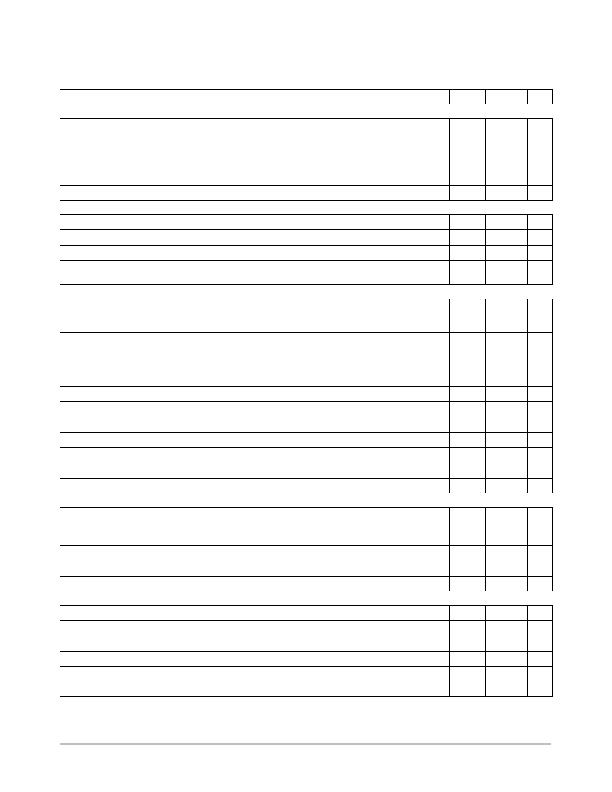
ELECTRICAL CHARACTERISTICS
(Unless otherwise specified: For typical values, T
J
= 25癈. For min/max values, T
J
= 40癈 to +125癈, V
CC
= 12 V, FB = 2.4 V, C
DRV
=
1 nF, Ct = 1 nF, CS = 0 V, Control = open, ZCD = open)
Symbol
Rating
Min
Typ
Max
Unit
V
CC
UNDERVOLTAGE LOCKOUT SECTION
V
CC(on)
V
CC
Startup Threshold (Undervoltage Lockout Threshold, Vcc rising)
25癈 < T
J
< +125癈
40癈 < T
J
< +125癈
11.0
10.9
12.0
12.0
13.0
13.1
V
V
CC(off)
V
CC
Disable Voltage after Turn On (Undervoltage Lockout Threshold, V
CC
falling)
25癈 < T
J
< +125癈
40癈 < T
J
< +125癈
8.7
8.5
9.5
9.5
10.3
10.5
V
H
UVLO
Undervoltage Lockout Hysteresis
2.2
2.5
2.8
V
DEVICE CONSUMPTION
I
CC(startup)
Icc consumption during startup: 0 V < V
CC
< V
CC(on)
200 mV
20
40
mA
I
CC1
Icc consumption after turn on at V
CC
= 12 V, No Load, 70 kHz switching
1.4
2.0
mA
I
CC2
Icc consumption after turn on at V
CC
= 12 V, 1 nF Load, 70 kHz switching
2.1
3
mA
I
CC(fault)
Icc consumption after turn on at V
CC
= 12 V, 1 nF Load, no switching
(such as during OVP fault, UVP fault, or grounding ZCD)
1.2
1.6
mA
REGULATION BLOCK (ERROR AMPLIFIER)
V
REF
Voltage Reference
@ T
J
= 25 癈
25癈 < T
J
< +125癈
40癈 < T
J
< +125癈
2.475
2.465
2.460
2.50
2.50
2.50
2.525
2.535
2.540
V
V
REF
(line)
Vref Line Regulation from V
CC(on)
+ 200 mV < V
CC
< 20 V, @ T
J
= 25癈
2
2
mV
I
EA
Error Amplifier Current Capability:: (Note 3)
Sink (Control = 4 V, V
FB
= 2.6 V):
Source (Control = 4 V, V
FB
= 2.4 V):
8.0
20
17
6.0
30
2
mA
G
OL
Open Loop, Error Amplifier Gain (Note 4)
80
dB
BW
Unity Gain Bandwidth (Note 4)
1
MHz
I
FB
FB Bias Current @ V
FB
= 3 V
500
500
nA
I
Control
Control Pin Bias Current @ FB = 0 V and Control = 4.0 V.
1
1
mA
V
EAH
V
CONTROL
@ I
EASOURCE
= 0.5 mA, V
FB
= 2.4 V
4.9
5.3
5.7
V
V
EAL
V
CONTROL
@ I
EASINK
= 0.5 mA, V
FB
= 2.6 V
1.85
2.1
2.4
V
V
EA
(diff)
V
EA
(diff) = V
EAH
V
EAL
. Difference between max and min Control voltages
3.0
3.2
3.4
V
CURRENT SENSE BLOCK
V
CS(limit)
Overcurrent Protection Threshold:
NCP1606A
NCP1606B
1.6
0.45
1.7
0.5
1.8
0.55
V
t
LEB
Leading Edge Blanking duration
150
250
350
ns
t
CS
Overcurrent protection propagation delay.
40
100
170
ns
I
CS
CS bias current @ V
CS
= 2 V
1
1
mA
ZERO CURRENT DETECTION
V
ZCDH
Zero Current Detection Threshold (V
ZCD
rising)
1.9
2.1
2.3
V
V
ZCDL
Zero Current Detection Threshold (V
ZCD
falling)
1.45
1.6
1.75
V
V
ZCD(HYS)
V
ZCD
H V
ZCD
L
300
500
800
mV
I
ZCD
Maximum ZCD bias Current @ V
ZCD
= 5 V
2
+2
mA
V
CL(POS)
Upper Clamp Voltage @ I
ZCD
= 2.5 mA
5
5.7
6.5
V
I
CL(POS)
Current Capability of the Positive Clamp at V
ZCD
= V
CL(POS)
+ 200 mV:
5.0
8.5
mA
3. Parameter values are valid for transient conditions only.
4. Parameter characterized and guaranteed by design, but not tested in production.
相关PDF资料 |
PDF描述 |
|---|---|
| NCP1607BDR2G | IC PFC CONTROLLER CRM 8SOIC |
| NCP1611BDR2G | IC PFC CTLR HE ENHANCED 8-SOIC |
| NCP1651DR2G | IC PFC CONTROLLER CCM/DCM 16SOIC |
| NCP1654BD133R2G | IC PFC CCM 133KHZ 8-SOIC |
| NCP1927DR2G | IC CTLR PFC/FLYBACK 16-SOIC |
相关代理商/技术参数 |
参数描述 |
|---|---|
| NCP1606BOOSTGEVB | 功能描述:电源管理IC开发工具 OSPI NCP1606 100 W BOOST RoHS:否 制造商:Maxim Integrated 产品:Evaluation Kits 类型:Battery Management 工具用于评估:MAX17710GB 输入电压: 输出电压:1.8 V |
| NCP1606BPG | 功能描述:功率因数校正 IC LO CST PWR FCTR CONT RoHS:否 制造商:Fairchild Semiconductor 开关频率:300 KHz 最大功率耗散: 最大工作温度:+ 125 C 安装风格:SMD/SMT 封装 / 箱体:SOIC-8 封装:Reel |
| NCP1607BDR2G | 功能描述:功率因数校正 IC CST EFCT PW FCTR CTR RoHS:否 制造商:Fairchild Semiconductor 开关频率:300 KHz 最大功率耗散: 最大工作温度:+ 125 C 安装风格:SMD/SMT 封装 / 箱体:SOIC-8 封装:Reel |
| NCP1607BOOSTGEVB | 功能描述:BOARD EVAL NCP1607 100W BOOST RoHS:是 类别:编程器,开发系统 >> 评估演示板和套件 系列:* 标准包装:1 系列:PCI Express® (PCIe) 主要目的:接口,收发器,PCI Express 嵌入式:- 已用 IC / 零件:DS80PCI800 主要属性:- 次要属性:- 已供物品:板 |
| NCP1608BDR2G | 功能描述:功率因数校正 IC COST EFFECT PWR FACT CONT RoHS:否 制造商:Fairchild Semiconductor 开关频率:300 KHz 最大功率耗散: 最大工作温度:+ 125 C 安装风格:SMD/SMT 封装 / 箱体:SOIC-8 封装:Reel |
发布紧急采购,3分钟左右您将得到回复。