- 您现在的位置:买卖IC网 > PDF目录22224 > NCP1910A65DWR2G (ON Semiconductor)IC COMBO CTLR ATX 24-SOIC PDF资料下载
参数资料
| 型号: | NCP1910A65DWR2G |
| 厂商: | ON Semiconductor |
| 文件页数: | 28/37页 |
| 文件大小: | 0K |
| 描述: | IC COMBO CTLR ATX 24-SOIC |
| 标准包装: | 1 |
| 模式: | 连续导电(CCM) |
| 频率 - 开关: | 245 kHz |
| 电流 - 启动: | 100µA |
| 安装类型: | 表面贴装 |
| 封装/外壳: | 24-SOIC(0.295",7.50mm 宽)23 引线 |
| 供应商设备封装: | 24-SOIC W |
| 包装: | 标准包装 |
| 其它名称: | NCP1910A65DWR2GOSDKR |
第1页第2页第3页第4页第5页第6页第7页第8页第9页第10页第11页第12页第13页第14页第15页第16页第17页第18页第19页第20页第21页第22页第23页第24页第25页第26页第27页当前第28页第29页第30页第31页第32页第33页第34页第35页第36页第37页
�� �
�
�NCP1910�
�maximum� sink� and� source� of� output� current� capability�
�of� OTA� is� around� 30� m� A.� Due� to� the� “V� out� Low� Detect”�
�block� (VLD),� when� the� V� FB� is� below� 95%� V� PREF� ,� an�
�extra� 200� m� A� current� source� (I� VLD� in� Figure� 52)� will�
�raise� V� CTRL� rapidly.� Hence� prevent� the� PFC� output�
�from� dropping� too� low� and� improve� the� transient�
�50�
�0�
�response� performance.� The� relationship� between�
�current� flowing� in/out� V� CTRL� pin� and� V� FB� is� as� shown�
�in� Figure� 53.�
�It� is� recommended� to� add� a� typical� 100� pF� capacitor� C� FB�
�decoupling� capacitor� next� to� feedback� pin� to� prevent� from�
�noise� impact.�
�?� 50� 2�
�2.2�
�2.4�
�2.6�
�2.8�
�3�
�?� 100�
�?� 150�
�?� 200�
�?� 250�
�230� m� A� raises� V� CTRL� rapidly�
�when� V� FB� is� below� 95%�
�V� PREF�
�No� DRV� when� V� FB� is�
�above� 105%� V� PREF�
�V� FB�
�Figure� 53.� V� FB� vs.� Current� Flowing� in/out� From� V� CTRL� Pin�
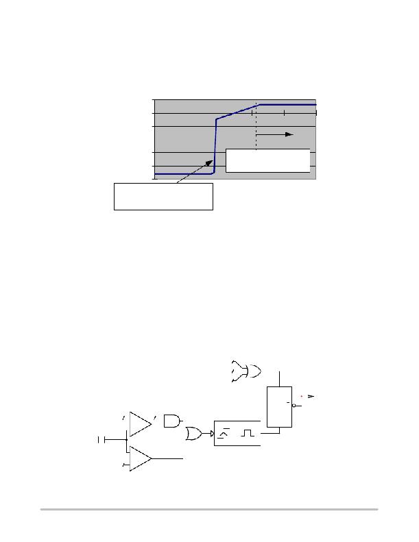
�PFCok� Signal�
�The� PFC� provides� a� “PFCok”� signal� to:�
�?� enable� the� dynamic� response� enhancer� (I� VLD� )� if� V� bulk� is�
�below� 95%,� finish� of� the� PFC� soft� ?� start,�
�?� enable� the� PFC� frequency� foldback,�
�?� enable� the� timer� (t� DEL1� ),� which� is� to� start� the� LLC� ?� HB�
�converter,�
�?� enable� the� timer� (t� DEL2� ),� which� is� to� stop� LLC� ?� HB�
�converter� once� “PFCok”� is� asserted� low� or� V� bulk� is�
�lower� than� PG� level� after� LLC� ?� HB� has� started.�
�Refer� to� Figure� 54.� “PFCok”� signal� is� low� when�
�?� the� PFC� stage� start� ?� up,� or�
�?� any� latch� off� signal� arrives,� or�
�?� line� brown� ?� out� activates.�
�“PFCok”� signal� is� high� when�
�?� DRV� starts� operating� and� the� PFC� stage� is� above� 95%�
�of� target,� i.e.� the� VLD� comparator� output� is� high,� or�
�?� the� PFC� stage� is� above� 100%� target,� i.e.� PFC� REG�
�comparator� output� is� high.�
�This� “PFCok”� signal� is� high� when� the� PFC� stage� is� in�
�normal� operation,� i.e.� its� output� is� above� 95%� of� normal�
�output,� and� low� otherwise.�
�PFC_BO�
�Latch�
�Grand� Reset�
�R�
�Q�
�Q�
�PFC_OK�
�95%� V� PREF�
�+�
�?�
�DRV�
�VLD�
�S�
�FB�
�+�
�V� PREF�
�?�
�PFC� REG�
�Figure� 54.� PFCok� Signal� Block� Diagram�
�http://onsemi.com�
�28�
�相关PDF资料 |
PDF描述 |
|---|---|
| SRR1280-221K | INDUCTOR POWER 220UH 1.60A SMD |
| EGM43DTMN | CONN EDGECARD 86POS R/A .156 SLD |
| T95R337K016LZSL | CAP TANT 330UF 16V 10% 2824 |
| RAC20-24SB | CONV AC/DC 20W 24V OUT SNGL T/H |
| VE-J4N-CX-F3 | CONVERTER MOD DC/DC 18.5V 75W |
相关代理商/技术参数 |
参数描述 |
|---|---|
| NCP1910B65DWR2G | 功能描述:交流/直流开关转换器 GREENM COMBO 2GND N/SKIP RoHS:否 制造商:STMicroelectronics 输出电压:800 V 输入/电源电压(最大值):23.5 V 输入/电源电压(最小值):11.5 V 开关频率:115 kHz 电源电流:1.6 mA 工作温度范围:- 40 C to + 150 C 安装风格:SMD/SMT 封装 / 箱体:SSO-10 封装:Reel |
| NCP1910GEVB | 功能描述:电源管理IC开发工具 NCP1910DEMO-B-TLS RoHS:否 制造商:Maxim Integrated 产品:Evaluation Kits 类型:Battery Management 工具用于评估:MAX17710GB 输入电压: 输出电压:1.8 V |
| NCP1927DR2G | 功能描述:功率因数校正 IC PFC AND FLYBACK CONTROLER RoHS:否 制造商:Fairchild Semiconductor 开关频率:300 KHz 最大功率耗散: 最大工作温度:+ 125 C 安装风格:SMD/SMT 封装 / 箱体:SOIC-8 封装:Reel |
| NCP1937A1DR2G | 制造商:ON Semiconductor 功能描述:COMBO PFC & QUAZI FLYBACK - Tape and Reel 制造商:ON Semiconductor 功能描述:REEL / COMBO PFC & QUAZI FLYBACK |
| NCP1937B1DR2G | 制造商:ON Semiconductor 功能描述:COMBO PFC & QUAZI FLYBACK - Tape and Reel |
发布紧急采购,3分钟左右您将得到回复。