- 您现在的位置:买卖IC网 > PDF目录22224 > NCP1910A65DWR2G (ON Semiconductor)IC COMBO CTLR ATX 24-SOIC PDF资料下载
参数资料
| 型号: | NCP1910A65DWR2G |
| 厂商: | ON Semiconductor |
| 文件页数: | 34/37页 |
| 文件大小: | 0K |
| 描述: | IC COMBO CTLR ATX 24-SOIC |
| 标准包装: | 1 |
| 模式: | 连续导电(CCM) |
| 频率 - 开关: | 245 kHz |
| 电流 - 启动: | 100µA |
| 安装类型: | 表面贴装 |
| 封装/外壳: | 24-SOIC(0.295",7.50mm 宽)23 引线 |
| 供应商设备封装: | 24-SOIC W |
| 包装: | 标准包装 |
| 其它名称: | NCP1910A65DWR2GOSDKR |
第1页第2页第3页第4页第5页第6页第7页第8页第9页第10页第11页第12页第13页第14页第15页第16页第17页第18页第19页第20页第21页第22页第23页第24页第25页第26页第27页第28页第29页第30页第31页第32页第33页当前第34页第35页第36页第37页
�� �
�
�NCP1910�
�LLC� High� ?� Voltage� Driver�
�The� NCP1910� includes� a� high� ?� voltage� driver� allowing� a�
�direct� connection� to� the� upper� side� MOSFET� of� LLC�
�converter.� This� device� also� incorporates� an� upper� UVLO�
�circuitry� that� makes� sure� enough� gate� voltage� is� available� for�
�the� upper� side� MOSFET.� The� bias� of� the� floating� driver�
�section� is� provided� by� C� boot� capacitor� between� V� boot� pin� and�
�HB� pin� that� is� refilled� by� external� booststrap� diode.� The�
�floating� portion� can� go� up� to� 600� Vdc� and� makes� the� IC�
�perfectly� suitable� for� offline� applications� featuring� a� 400� V�
�PFC� front� ?� end� stage.�
�Combo� Management� Section�
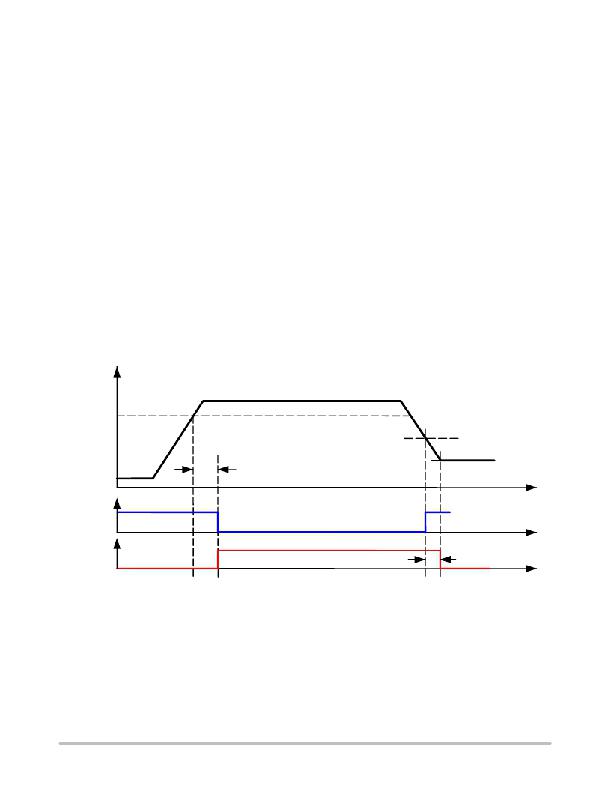
�Start� ?� up� and� Stop� Delay� of� LLC� and� Pgout� signal�
�(t� DEL1� and� t� DEL2� )�
�To� ensure� the� proper� operation� of� LLC,� LLC� cannot� start�
�if� the� PFC� is� not� ready.�
�As� depicted� in� the� “PFCok� signal”� section,� the� internal�
�PFCok� signal� is� asserted� high� when� V� bulk� is� above� 95%� of�
�normal� bulk� voltage.� After� PFCok� signal� is� high,� a� timer�
�(t� DEL1� )� starts� to� ensure� PFC� stage� is� fully� stable� before� LLC�
�starts.� When� t� DEL1� is� elapsed,� PG� out� pin� is� grounded� and�
�LLC� starts� its� driver� outputs� (ML� and� MU� pins).�
�another� timer� (t� DEL2� )� starts.� Once� the� t� DEL2� is� elapsed,� LLC�
�stops� its� drivers� (ML� and� MU� pins).�
�Figure� 61� depicts� the� start� ?� up� and� stop� delay� of� LLC� and�
�PG� out� .�
�Once� the� PFC� is� ready� (PFCok� is� asserted� high),� t� DEL1�
�(20� ms� typically)� is� started.� Once� this� delay� is� elapsed:�
�?� PG� out� pin� is� asserted� low�
�?� LLC� drivers� (ML� and� MU� pins)� can� start� to� operate.�
�As� shutdown� by� unplug� ac� input,� V� bulk� decreases:�
�?� When� it� reaches� the� PG� signal,� which� is� adjusted� by�
�PG� adj� pin,� PG� out� pin� is� released� open.�
�?� If� V� bulk� reaches� the� LLC� stop� level� (BO� level� adjusted�
�by� BO� adj� pin),� the� LLC� stops;� or� if� V� bulk� drops� slowly,�
�e.g.� light� load,� LLC� drivers� (ML� and� MU� pins)� will�
�stop� 5� ms� after� PG� out� pin� is� released� (t� DEL2� ).�
�As� shutdown� by� line� brown� ?� out� situation,� PFCok� signal� will�
�be� pulled� down:�
�?� PG� out� pin� is� released� open� once� this� internal� PFCok�
�signal� is� low.�
�?� LLC� drivers� (ML� and� MU� pins)� will� stop� 5� ms� after�
�PG� out� pin� is� released� open� (t� DEL2� ).�
�In� case� of� shutdown� by� unplugging� ac� input� or� line� brown�
�out� situation,� PG� out� signal� is� released� open.� And� then�
�V� bulk�
�95%�
�PG� level�
�t� DEL1�
�BO� level�
�20� ms�
�PG� out�
�t� DEL2�
�LLC� works�
�off�
�5� ms�
�Figure� 61.� The� Timing� for� t� DEL1� and� t� DEL2�
�off�
�time�
�Remote� on/off� (on/off� pin)�
�NCP1910� reserves� one� dedicated� pin� for� remote� control�
�feature� at� on/off� pin:�
�?� When� the� on/off� pin� is� pulled� below� 1� V,� the� PFC� starts�
�operation.� 20� ms� after� V� bulk� is� above� 95%� of� target�
�level,� LLC� starts.�
�?� When� the� on/off� pin� is� above� 3� V,� the� device� stops� both�
�PFC� and� LLC� immediately� and� keeps� low�
�consumption.� Figure� 62� depicts� the� relationship�
�between� the� operation� mode� and� on/off� pin.�
�http://onsemi.com�
�34�
�相关PDF资料 |
PDF描述 |
|---|---|
| SRR1280-221K | INDUCTOR POWER 220UH 1.60A SMD |
| EGM43DTMN | CONN EDGECARD 86POS R/A .156 SLD |
| T95R337K016LZSL | CAP TANT 330UF 16V 10% 2824 |
| RAC20-24SB | CONV AC/DC 20W 24V OUT SNGL T/H |
| VE-J4N-CX-F3 | CONVERTER MOD DC/DC 18.5V 75W |
相关代理商/技术参数 |
参数描述 |
|---|---|
| NCP1910B65DWR2G | 功能描述:交流/直流开关转换器 GREENM COMBO 2GND N/SKIP RoHS:否 制造商:STMicroelectronics 输出电压:800 V 输入/电源电压(最大值):23.5 V 输入/电源电压(最小值):11.5 V 开关频率:115 kHz 电源电流:1.6 mA 工作温度范围:- 40 C to + 150 C 安装风格:SMD/SMT 封装 / 箱体:SSO-10 封装:Reel |
| NCP1910GEVB | 功能描述:电源管理IC开发工具 NCP1910DEMO-B-TLS RoHS:否 制造商:Maxim Integrated 产品:Evaluation Kits 类型:Battery Management 工具用于评估:MAX17710GB 输入电压: 输出电压:1.8 V |
| NCP1927DR2G | 功能描述:功率因数校正 IC PFC AND FLYBACK CONTROLER RoHS:否 制造商:Fairchild Semiconductor 开关频率:300 KHz 最大功率耗散: 最大工作温度:+ 125 C 安装风格:SMD/SMT 封装 / 箱体:SOIC-8 封装:Reel |
| NCP1937A1DR2G | 制造商:ON Semiconductor 功能描述:COMBO PFC & QUAZI FLYBACK - Tape and Reel 制造商:ON Semiconductor 功能描述:REEL / COMBO PFC & QUAZI FLYBACK |
| NCP1937B1DR2G | 制造商:ON Semiconductor 功能描述:COMBO PFC & QUAZI FLYBACK - Tape and Reel |
发布紧急采购,3分钟左右您将得到回复。