- 您现在的位置:买卖IC网 > PDF目录22224 > NCP1910A65DWR2G (ON Semiconductor)IC COMBO CTLR ATX 24-SOIC PDF资料下载
参数资料
| 型号: | NCP1910A65DWR2G |
| 厂商: | ON Semiconductor |
| 文件页数: | 37/37页 |
| 文件大小: | 0K |
| 描述: | IC COMBO CTLR ATX 24-SOIC |
| 标准包装: | 1 |
| 模式: | 连续导电(CCM) |
| 频率 - 开关: | 245 kHz |
| 电流 - 启动: | 100µA |
| 安装类型: | 表面贴装 |
| 封装/外壳: | 24-SOIC(0.295",7.50mm 宽)23 引线 |
| 供应商设备封装: | 24-SOIC W |
| 包装: | 标准包装 |
| 其它名称: | NCP1910A65DWR2GOSDKR |
第1页第2页第3页第4页第5页第6页第7页第8页第9页第10页第11页第12页第13页第14页第15页第16页第17页第18页第19页第20页第21页第22页第23页第24页第25页第26页第27页第28页第29页第30页第31页第32页第33页第34页第35页第36页当前第37页
��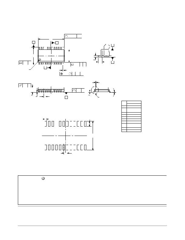 �
�
�NCP1910�
�PACKAGE� DIMENSIONS�
�A1�
�CASE� 752AB� ?� 01�
�ISSUE� O�
�E1�
�B�
�DETAIL� A�
�e�
�c�
�C�
�DETAIL� A�
�D�
�E�
�2X�
�0.33� C�
�PIN� 1�
�INDICATOR�
�0.10� C�
�A�
�NOTE� 8�
�24�
�1�
�SOIC� ?� 24� WB� LESS� PIN� 21�
�2X�
�0.20� C� A-B�
�D�
�A�
�NOTE� 7�
�13�
�NOTES� 5� &� 6�
�12� L2�
�L�
�0.10� C� D�
�2X�
�NOTE� 7� 24X� b�
�0.25� M� C� A-B� D�
�TOP� VIEW� NOTES� 3� &� 4�
�NOTE� 9�
�h�
�x� 45� _�
�0.10� C�
�SEATING�
�PLANE�
�SIDE� VIEW� END� VIEW�
�RECOMMENDED�
�SOLDERING� FOOTPRINT*�
�23X�
�23X�
�1.62�
�0.52�
�H�
�C�
�M�
�NOTES:�
�1.� DIMENSIONING� AND� TOLERANCING� PER� ASME�
�Y14.5M,� 1994.�
�2.� CONTROLLING� DIMENSION:� MILLIMETERS.�
�3.� DIMENSION� B� DOES� NOT� INCLUDE� DAMBAR�
�PROTRUSION.� ALLOWABLE� PROTRUSION� SHALL�
�BE� 0.10� mm� TOTAL� IN� EXCESS� OF� ’b’� AT� MAXIM-�
�UM� MATERIAL� CONDITION.�
�4.� DIMENSIONS� b� AND� c� APPLY� TO� THE� FLAT� SEC-�
�TION� OF� THE� LEAD� AND� ARE� MEASURED�
�BETWEEN� 0.10� AND� 0.25� FROM� THE� LEAD� TIP.�
�5.� DIMENSIONS� D� AND� E1� DO� NOT� INCLUDE� MOLD�
�FLASH,� PROTRUSIONS� OR� GATE� BURRS.� MOLD�
�FLASH,� PROTRUSIONS� OR� GATE� BURRS� SHALL�
�NOT� EXCEED� 0.15� mm� PER� SIDE.� INTERLEAD�
�FLASH� OR� PROTRUSION� SHALL� NOT� EXCEED�
�0.25� PER� SIDE.� DIMENSIONS� D� AND� E1� ARE�
�DETERMINED� AT� DATUM� H.�
�6.� DIMENSIONS� D� AND� E1� ARE� DETERMINED� AT�
�THE� OUTERMOST� EXTREMES� OF� THE� PLASTIC�
�BODY� EXCLUSIVE� OF� MOLD� FLASH,�
�PROTRUSIONS,� TIE� BAR� BURRS,� OR� GATE�
�BURRS� BUT� INCLUSIVE� OF� ANY� MOLD�
�MISMATCH� BETWEEN� THE� TOP� AND� BOTTOM� OF�
�THE� PLASTIC� BODY.�
�7.� DIMENSIONS� A� AND� B� ARE� TO� BE� DETERMINED�
�AT� DATUM� H.�
�8.� A1� IS� DEFINED� AS� THE� VERTICAL� DISTANCE�
�FROM� THE� SEATING� PLANE� TO� THE� LOWEST�
�POINT� ON� THE� PACKAGE� BODY.�
�9.� THIS� CHAMFER� IS� OPTIONAL.� IF� IT� IS� NOT�
�PRESENT,� THEN� A� PIN� 1� IDENTIFIER� MUST� BE�
�LOCATED� IN� THE� INDICATED� AREA.�
�MILLIMETERS�
�DIM�
�MIN� MAX�
�2.35� 2.65�
�A�
�0.10� 0.29�
�A1�
�0.31� 0.51�
�b�
�0.20� 0.33�
�J�
�15.40� BSC�
�D�
�10.30� BSC�
�E�
�7.50� BSC�
�E1�
�11.00�
�e�
�h�
�L�
�L2�
�M�
�1.27� BSC�
�0.25� 0.75�
�0.40� 1.27�
�0.25� BSC�
�0� _� 8� _�
�1�
�1.27�
�PITCH�
�DIMENSIONS:� MILLIMETERS�
�*For� additional� information� on� our� Pb� ?� Free� strategy� and� soldering�
�details,� please� download� the� ON� Semiconductor� Soldering� and�
�Mounting� Techniques� Reference� Manual,� SOLDERRM/D.�
�ON� Semiconductor� and� are� registered� trademarks� of� Semiconductor� Components� Industries,� LLC� (SCILLC).� SCILLC� owns� the� rights� to� a� number� of� patents,� trademarks,�
�copyrights,� trade� secrets,� and� other� intellectual� property.� A� listing� of� SCILLC’s� product/patent� coverage� may� be� accessed� at� www.onsemi.com/site/pdf/Patent� ?� Marking.pdf.� SCILLC�
�reserves� the� right� to� make� changes� without� further� notice� to� any� products� herein.� SCILLC� makes� no� warranty,� representation� or� guarantee� regarding� the� suitability� of� its� products� for� any�
�particular� purpose,� nor� does� SCILLC� assume� any� liability� arising� out� of� the� application� or� use� of� any� product� or� circuit,� and� specifically� disclaims� any� and� all� liability,� including� without�
�limitation� special,� consequential� or� incidental� damages.� “Typical”� parameters� which� may� be� provided� in� SCILLC� data� sheets� and/or� specifications� can� and� do� vary� in� different� applications�
�and� actual� performance� may� vary� over� time.� All� operating� parameters,� including� “Typicals”� must� be� validated� for� each� customer� application� by� customer’s� technical� experts.� SCILLC�
�does� not� convey� any� license� under� its� patent� rights� nor� the� rights� of� others.� SCILLC� products� are� not� designed,� intended,� or� authorized� for� use� as� components� in� systems� intended� for�
�surgical� implant� into� the� body,� or� other� applications� intended� to� support� or� sustain� life,� or� for� any� other� application� in� which� the� failure� of� the� SCILLC� product� could� create� a� situation� where�
�personal� injury� or� death� may� occur.� Should� Buyer� purchase� or� use� SCILLC� products� for� any� such� unintended� or� unauthorized� application,� Buyer� shall� indemnify� and� hold� SCILLC� and�
�its� officers,� employees,� subsidiaries,� affiliates,� and� distributors� harmless� against� all� claims,� costs,� damages,� and� expenses,� and� reasonable� attorney� fees� arising� out� of,� directly� or� indirectly,�
�any� claim� of� personal� injury� or� death� associated� with� such� unintended� or� unauthorized� use,� even� if� such� claim� alleges� that� SCILLC� was� negligent� regarding� the� design� or� manufacture�
�of� the� part.� SCILLC� is� an� Equal� Opportunity/Affirmative� Action� Employer.� This� literature� is� subject� to� all� applicable� copyright� laws� and� is� not� for� resale� in� any� manner.�
�PUBLICATION� ORDERING� INFORMATION�
�LITERATURE� FULFILLMENT� :�
�Literature� Distribution� Center� for� ON� Semiconductor�
�P.O.� Box� 5163,� Denver,� Colorado� 80217� USA�
�Phone� :� 303� ?� 675� ?� 2175� or� 800� ?� 344� ?� 3860� Toll� Free� USA/Canada�
�Fax� :� 303� ?� 675� ?� 2176� or� 800� ?� 344� ?� 3867� Toll� Free� USA/Canada�
�Email� :� orderlit@onsemi.com�
�N.� American� Technical� Support� :� 800� ?� 282� ?� 9855� Toll� Free�
�USA/Canada�
�Europe,� Middle� East� and� Africa� Technical� Support:�
�Phone:� 421� 33� 790� 2910�
�Japan� Customer� Focus� Center�
�Phone:� 81� ?� 3� ?� 5817� ?� 1050�
�http://onsemi.com�
�37�
�ON� Semiconductor� Website� :� www.onsemi.com�
�Order� Literature� :� http://www.onsemi.com/orderlit�
�For� additional� information,� please� contact� your� local�
�Sales� Representative�
�NCP1910/D�
�相关PDF资料 |
PDF描述 |
|---|---|
| SRR1280-221K | INDUCTOR POWER 220UH 1.60A SMD |
| EGM43DTMN | CONN EDGECARD 86POS R/A .156 SLD |
| T95R337K016LZSL | CAP TANT 330UF 16V 10% 2824 |
| RAC20-24SB | CONV AC/DC 20W 24V OUT SNGL T/H |
| VE-J4N-CX-F3 | CONVERTER MOD DC/DC 18.5V 75W |
相关代理商/技术参数 |
参数描述 |
|---|---|
| NCP1910B65DWR2G | 功能描述:交流/直流开关转换器 GREENM COMBO 2GND N/SKIP RoHS:否 制造商:STMicroelectronics 输出电压:800 V 输入/电源电压(最大值):23.5 V 输入/电源电压(最小值):11.5 V 开关频率:115 kHz 电源电流:1.6 mA 工作温度范围:- 40 C to + 150 C 安装风格:SMD/SMT 封装 / 箱体:SSO-10 封装:Reel |
| NCP1910GEVB | 功能描述:电源管理IC开发工具 NCP1910DEMO-B-TLS RoHS:否 制造商:Maxim Integrated 产品:Evaluation Kits 类型:Battery Management 工具用于评估:MAX17710GB 输入电压: 输出电压:1.8 V |
| NCP1927DR2G | 功能描述:功率因数校正 IC PFC AND FLYBACK CONTROLER RoHS:否 制造商:Fairchild Semiconductor 开关频率:300 KHz 最大功率耗散: 最大工作温度:+ 125 C 安装风格:SMD/SMT 封装 / 箱体:SOIC-8 封装:Reel |
| NCP1937A1DR2G | 制造商:ON Semiconductor 功能描述:COMBO PFC & QUAZI FLYBACK - Tape and Reel 制造商:ON Semiconductor 功能描述:REEL / COMBO PFC & QUAZI FLYBACK |
| NCP1937B1DR2G | 制造商:ON Semiconductor 功能描述:COMBO PFC & QUAZI FLYBACK - Tape and Reel |
发布紧急采购,3分钟左右您将得到回复。