参数资料
| 型号: | NCP5331FTR2 |
| 厂商: | ON Semiconductor |
| 文件页数: | 14/36页 |
| 文件大小: | 0K |
| 描述: | IC CTRLR BUCK 2PH PWM DRV 32LQFP |
| 产品变化通告: | Product Obsolescence 11/Feb/2009 |
| 标准包装: | 1 |
| 应用: | 控制器,AMD Athlon? |
| 输入电压: | 9 V ~ 14 V |
| 输出数: | 2 |
| 输出电压: | 5V |
| 工作温度: | 0°C ~ 70°C |
| 安装类型: | 表面贴装 |
| 封装/外壳: | 32-LQFP |
| 供应商设备封装: | 32-LQFP(7x7) |
| 包装: | 剪切带 (CT) |
| 其它名称: | NCP5331FTR2OSCT |
第1页第2页第3页第4页第5页第6页第7页第8页第9页第10页第11页第12页第13页当前第14页第15页第16页第17页第18页第19页第20页第21页第22页第23页第24页第25页第26页第27页第28页第29页第30页第31页第32页第33页第34页第35页第36页
�� �
�
�NCP5331�
�APPLICATIONS� INFORMATION�
�Overview�
�The� NCP5331� dc/dc� controller� utilizes� an� Enhanced� V� 2�
�topology� to� meet� requirements� of� low� voltage,� high� current�
�loads� with� fast� transient� requirements.� Transient� response�
�has� been� improved� and� voltage� jitter� virtually� eliminated� by�
�including� an� internal� PWM� ramp,� connecting� fast?feedback�
�from� V� CORE� directly� to� the� internal� PWM� comparator,� and�
�precise� routing� and� grounding� inside� the� controller.�
�Advanced� features� such� as� adjustable� power?good� delay,�
�programmable� overcurrent� shutdown� time,� superior�
�overvoltage� protection� (OVP),� and� differential� remote�
�voltage� sensing� make� it� easy� to� obtain� AMD� certification.�
�An� innovative� overvoltage� protection� (OVP)� scheme�
�safeguards� the� CPU� during� extreme� situations� including�
�power� up� with� a� shorted� upper� MOSFET,� shorting� of� an�
�upper� MOSFET� during� normal� operation,� and� loss� of� the�
�voltage� feedback� signal,� COREFB+.� The� NCP5331�
�provides� a� “fully� integrated� solution”� to� simplify� design,�
�minimize� circuit� board� area,� and� reduce� overall� system� cost.�
�Two� advantages� of� a� multiphase� converter� over� a�
�single?phase� converter� are� current� sharing� and� increased�
�apparent� output� frequency.� Current� sharing� allows� the�
�designer� to� use� less� inductance� in� each� phase� than� would� be�
�required� in� a� single?phase� converter.� The� smaller� inductor�
�produces� larger� ripple� currents� but� the� total� per� phase� power�
�dissipation� is� reduced� because� the� rms� current� is� lower.�
�Transient� response� is� improved� because� the� control� loop� will�
�measure� and� adjust� the� current� faster� in� a� smaller� output�
�inductor.� Increased� apparent� output� frequency� is� desirable�
�because� the� off?time� and� the� ripple� voltage� of� the� two?phase�
�converter� will� be� less� than� that� of� a� single?phase� converter.�
�Fixed� Frequency� Multiphase� Control�
�In� a� multiphase� converter,� multiple� converters� are�
�connected� in� parallel� and� are� switched� on� at� different� times.�
�This� reduces� output� current� from� the� individual� converters�
�and� increases� the� apparent� ripple� frequency.� Because� several�
�converters� are� connected� in� parallel,� output� current� can� ramp�
�up� or� down� faster� than� a� single� converter� (with� the� same�
�value� output� inductor)� and� heat� is� spread� among� multiple�
�components.�
�The� NCP5331� controller� uses� a� two?phase,� fixed�
�frequency,� Enhanced� V� 2� architecture� to� measure� and� control�
�currents� in� individual� phases.� Each� phase� is� delayed� 180� °�
�from� the� previous� phase.� Normally,� GHx� (x� =� 1� or� 2)�
�transitions� to� a� high� voltage� at� the� beginning� of� each�
�oscillator� cycle.� Inductor� current� ramps� up� until� the�
�combination� of� the� current� sense� signal,� the� internal� ramp�
�and� the� output� voltage� ripple� trip� the� PWM� comparator� and�
�bring� GHx� low.� Once� GHx� goes� low,� it� will� remain� low� until�
�the� beginning� of� the� next� oscillator� cycle.� While� GHx� is�
�high,� the� Enhanced� V� 2� loop� will� respond� to� line� and� load�
�variations� (i.e.� the� upper� gate� on?time� will� be� increased� or�
�reduced� as� required).� On� the� other� hand,� once� GHx� is� low,�
�the� loop� can� not� respond� until� the� beginning� of� the� next�
�PWM� cycle.� Therefore,� constant� frequency� Enhanced� V� 2�
�will� typically� respond� to� disturbances� within� the� off?time� of�
�the� converter.�
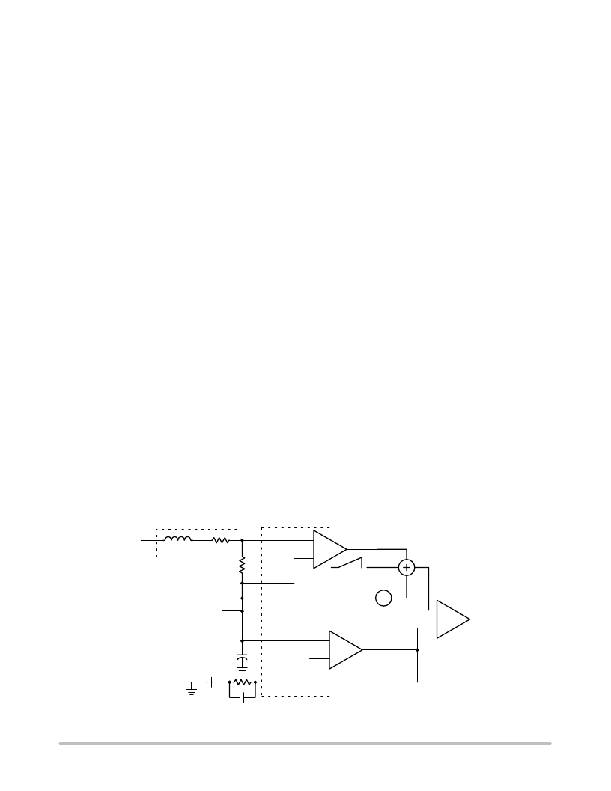
�The� Enhanced� V� 2� architecture� measures� and� adjusts� the�
�output� current� in� each� phase.� An� additional� input,� CSx� (x� =�
�1� or� 2),� for� inductor� current� information� has� been� added� to� the�
�V� 2� loop� for� each� phase� as� shown� in� Figure� 14.� The� triangular�
�inductor� current� is� measured� differentially� across� RS,�
�amplified� by� CSA� and� summed� with� the� Channel� Startup�
�Offset,� the� Internal� Ramp,� and� the� Output� Voltage� at� the�
�noninverting� input� of� the� PWM� comparator.� The� purpose� of�
�the� Internal� Ramp� is� to� compensate� for� propagation� delays� in�
�the� NCP5331.� This� provides� greater� design� flexibility� by�
�allowing� smaller� external� ramps,� lower� minimum� pulse�
�widths,� higher� frequency� operation,� and� PWM� duty� cycles�
�above� 50%� without� external� slope� compensation.� As� the� sum�
�of� the� inductor� current� and� the� internal� ramp� increase,� the�
�voltage� on� the� positive� pin� of� the� PWM� comparator� rises� and�
�terminates� the� PWM� cycle.� If� the� inductor� starts� a� cycle�
�SWNODE�
�Lx�
�RLx�
�CSx�
�x� =� 1� or� 2�
�+�
�CSA�
�COn�
�?�
�RSx�
�CS� REF�
�Internal� Ramp�
�V� OUT�
�(V� CORE� )�
�V� FFB�
�V� FB�
�“Fast?Feedback”�
�Connection�
�?�
�?+�
�Channel�
�Start?Up�
�Offset�
�+�
�?�
�PWM�
�To� F/F�
�Reset�
�+�
�DAC�
�Out�
�+�
�Error�
�COMP�
�COMP�
�Amp�
�Figure� 14.� Enhanced� V� 2� Control� Employing� Resistive� Current� Sensing� and� Additional� Internal� Ramp�
�http://onsemi.com�
�14�
�相关PDF资料 |
PDF描述 |
|---|---|
| RSM25DTBN | CONN EDGECARD 50POS R/A .156 SLD |
| P1812R-274K | INDUCTOR POWER 270UH SMD |
| UUR1E331MNL6GS | CAP ALUM 330UF 25V 20% SMD |
| X4323V8 | IC SUPERVISOR CPU 32K EE 8-TSSOP |
| NCP5322ADWR2 | IC CTRLR BUCK 2PH STEPDWN 28SOIC |
相关代理商/技术参数 |
参数描述 |
|---|---|
| NCP5331FTR2G | 功能描述:DC/DC 开关控制器 2 Phase Buck w/Gate Drivers for Athlon RoHS:否 制造商:Texas Instruments 输入电压:6 V to 100 V 开关频率: 输出电压:1.215 V to 80 V 输出电流:3.5 A 输出端数量:1 最大工作温度:+ 125 C 安装风格: 封装 / 箱体:CPAK |
| NCP5332A | 制造商:ONSEMI 制造商全称:ON Semiconductor 功能描述:Two-Phase Buck Controller with Integrated Gate Drivers and 5-Bit DAC |
| NCP5332A/D | 制造商:ONSEMI 制造商全称:ON Semiconductor 功能描述:Two-Phase Buck Controller with Integrated Gate Drivers and 5-Bit DAC |
| NCP5332ADW | 功能描述:DC/DC 开关控制器 2 Phase Buck w/Gate RoHS:否 制造商:Texas Instruments 输入电压:6 V to 100 V 开关频率: 输出电压:1.215 V to 80 V 输出电流:3.5 A 输出端数量:1 最大工作温度:+ 125 C 安装风格: 封装 / 箱体:CPAK |
| NCP5332ADWR2 | 功能描述:DC/DC 开关控制器 2 Phase Buck w/Gate RoHS:否 制造商:Texas Instruments 输入电压:6 V to 100 V 开关频率: 输出电压:1.215 V to 80 V 输出电流:3.5 A 输出端数量:1 最大工作温度:+ 125 C 安装风格: 封装 / 箱体:CPAK |
发布紧急采购,3分钟左右您将得到回复。