参数资料
| 型号: | NCP5331FTR2 |
| 厂商: | ON Semiconductor |
| 文件页数: | 15/36页 |
| 文件大小: | 0K |
| 描述: | IC CTRLR BUCK 2PH PWM DRV 32LQFP |
| 产品变化通告: | Product Obsolescence 11/Feb/2009 |
| 标准包装: | 1 |
| 应用: | 控制器,AMD Athlon? |
| 输入电压: | 9 V ~ 14 V |
| 输出数: | 2 |
| 输出电压: | 5V |
| 工作温度: | 0°C ~ 70°C |
| 安装类型: | 表面贴装 |
| 封装/外壳: | 32-LQFP |
| 供应商设备封装: | 32-LQFP(7x7) |
| 包装: | 剪切带 (CT) |
| 其它名称: | NCP5331FTR2OSCT |
第1页第2页第3页第4页第5页第6页第7页第8页第9页第10页第11页第12页第13页第14页当前第15页第16页第17页第18页第19页第20页第21页第22页第23页第24页第25页第26页第27页第28页第29页第30页第31页第32页第33页第34页第35页第36页
�� �
�
�NCP5331�
�SWNODE�
�Lx�
�RSx�
�CSx�
�x� =� 1� or� 2�
�+�
�CSA�
�?�
�COn�
�RLx�
�CSx�
�CS� REF�
�Internal� Ramp�
�V� OUT�
�(V� CORE� )�
�V� FFB�
�V� FB�
�“Fast?Feedback”�
�Connection�
�?�
�?+�
�Channel�
�Start?Up�
�Offset�
�+�
�?�
�PWM�
�To� F/F�
�Reset�
�+�
�DAC�
�Out�
�+�
�Error�
�COMP�
�COMP�
�Amp�
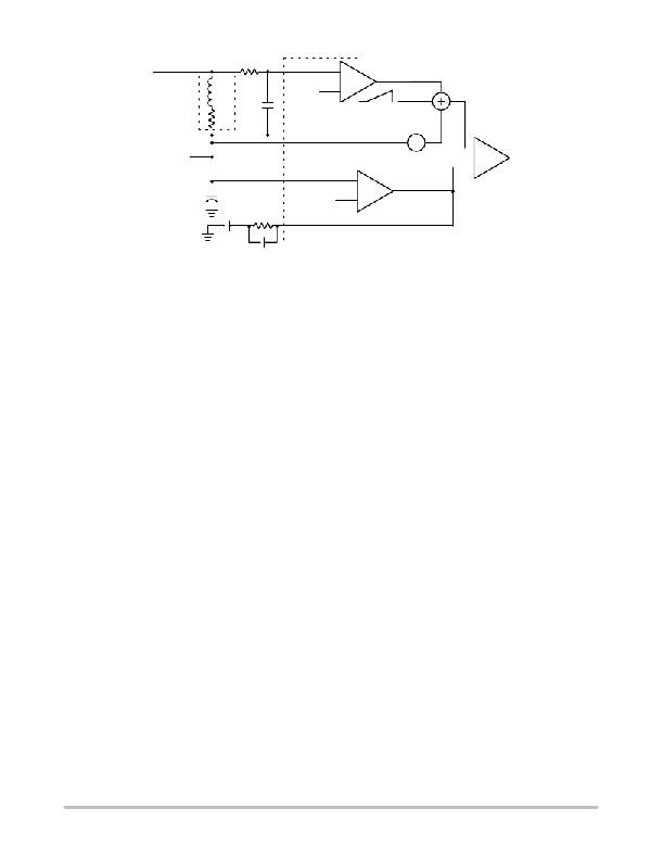
�Figure� 15.� Enhanced� V� 2� Control� Employing� Lossless� Inductive� Current� Sensing� and� Internal� Ramp�
�with� higher� current,� the� PWM� cycle� will� terminate� earlier�
�providing� negative� feedback.� The� NCP5331� provides� a� CSx�
�input� for� each� phase,� but� the� CS� REF� and� COMP� inputs� are�
�common� to� all� phases.� Current� sharing� is� accomplished� by�
�referencing� all� phases� to� the� same� CS� REF� and� COMP� pins,�
�so� that� a� phase� with� a� larger� current� signal� will� turn� off� earlier�
�than� a� phase� with� a� smaller� current� signal.�
�Enhanced� V� 2� responds� to� disturbances� in� V� CORE� by�
�employing� both� “slow”� and� “fast”� voltage� regulation.� The�
�internal� error� amplifier� performs� the� slow� regulation.�
�Depending� on� the� gain� and� frequency� compensation� set� by�
�the� amplifier� ’s� external� components,� the� error� amplifier� will�
�typically� begin� to� ramp� its� output� to� react� to� changes� in� the�
�output� voltage� in� 1?2� PWM� cycles.� Fast� voltage� feedback� is�
�implemented� by� a� direct� connection� from� V� CORE� to� the�
�noninverting� pin� of� the� PWM� comparator� via� the� summation�
�with� the� inductor� current,� internal� ramp,� and� the� Startup�
�OFFSET.� A� rapid� increase� in� load� current� will� produce� a�
�negative� offset� at� V� CORE� and� at� the� output� of� the� summer.�
�This� will� cause� the� PWM� duty� cycle� to� increase� almost�
�instantly.� Fast� feedback� will� typically� adjust� the� PWM� duty�
�cycle� within� 1� PWM� cycle.�
�As� shown� in� Figure� 14,� an� internal� ramp� (nominally� 125� mV�
�at� a� 50%� duty� cycle)� is� added� to� the� inductor� current� ramp� at�
�the� positive� terminal� of� the� PWM� comparator.� This� additional�
�ramp� compensates� for� propagation� time� delays� from� the�
�current� sense� amplifier� (CSA),� the� PWM� comparator,� and� the�
�MOSFET� gate� drivers.� As� a� result,� the� minimum� ON� time� of�
�the� controller� is� reduced� and� lower� duty� cycles� may� be�
�achieved� at� higher� frequencies.� Also,� the� additional� ramp�
�reduces� the� reliance� on� the� inductor� current� ramp� and� allows�
�greater� flexibility� when� choosing� the� output� inductor� and� the�
�RSxCSx� (x� =� 1� or� 2)� time� constant� (see� Figure� 15)� of� the�
�feedback� components� from� V� CORE� to� the� CSx� pin.�
�Including� both� current� and� voltage� information� in� the�
�feedback� signal� allows� the� open� loop� output� impedance� of�
�the� power� stage� to� be� controlled.� When� the� average� output�
�VCOMP� +� VCORE� @� 0� A� )� Channel_Startup_Offset�
�)� Int_Ramp� )� GCSA� @� Ext_Ramp� 2�
�Int_Ramp� is� the� internal� ramp� value� at� the� corresponding�
�duty� cycle,� Ext_Ramp� is� the� peak?to?peak� external�
�steady?state� ramp� at� 0� A,� G� CSA� is� the� Current� Sense�
�Amplifier� Gain� (nominally� 2.0� V/V),� and� the� Startup� Offset�
�is� typically� 0.60� V.� The� magnitude� of� the� Ext_Ramp� can� be�
�calculated� from�
�Ext_Ramp� +� D� @� (VIN� *� VCORE)� (RSx� @� CSx� @� fSW)�
�For� example,� if� V� CORE� at� 0� A� is� set� to� 1.225� V� with� AVP�
�and� the� input� voltage� is� 12.0� V,� the� duty� cycle� (D)� will� be�
�1.225/12.0� or� 10.2%.� Int_Ramp� will� be� 125� mV� ?� 10.2/50� =�
�25.5� mV.� Realistic� values� for� RSx,� CSx� and� f� SW� are� 5.6� k� W� ,�
�0.1� m� F,� and� 200� kHz� ?� using� these� and� the� previously�
�mentioned� formula,� Ext_Ramp� will� be� 9.8� mV.�
�VCOMP� +� 1.225� V� )� 0.60� V� )� 25.5� mV�
�)� 2.0� V� V� @� 9.8� mV� 2�
�+� 1.855� Vdc.�
�If� the� COMP� pin� is� held� steady� and� the� inductor� current�
�changes,� there� must� also� be� a� change� in� the� output� voltage.�
�Or,� in� a� closed� loop� configuration� when� the� output� current�
�changes,� the� COMP� pin� must� move� to� keep� the� same� output�
�voltage.� The� required� change� in� the� output� voltage� or� COMP�
�pin� depends� on� the� scaling� of� the� current� feedback� signal� and�
�is� calculated� as�
�D� V� +� RSx� @� GCSA� @� D� IOUT.�
�The� single?phase� power� stage� output� impedance� is�
�Single� Stage� Impedance� +� D� VOUT� D� IOUT� +� RS� @� GCSA�
�The� multiphase� power� stage� output� impedance� is� the�
�single?phase� output� impedance� divided� by� the� number� of�
�phases.� The� output� impedance� of� the� power� stage� determines�
�how� the� converter� will� respond� during� the� first� few�
�current� is� zero,� the� COMP� pin� will� be�
�http://onsemi.com�
�15�
�相关PDF资料 |
PDF描述 |
|---|---|
| RSM25DTBN | CONN EDGECARD 50POS R/A .156 SLD |
| P1812R-274K | INDUCTOR POWER 270UH SMD |
| UUR1E331MNL6GS | CAP ALUM 330UF 25V 20% SMD |
| X4323V8 | IC SUPERVISOR CPU 32K EE 8-TSSOP |
| NCP5322ADWR2 | IC CTRLR BUCK 2PH STEPDWN 28SOIC |
相关代理商/技术参数 |
参数描述 |
|---|---|
| NCP5331FTR2G | 功能描述:DC/DC 开关控制器 2 Phase Buck w/Gate Drivers for Athlon RoHS:否 制造商:Texas Instruments 输入电压:6 V to 100 V 开关频率: 输出电压:1.215 V to 80 V 输出电流:3.5 A 输出端数量:1 最大工作温度:+ 125 C 安装风格: 封装 / 箱体:CPAK |
| NCP5332A | 制造商:ONSEMI 制造商全称:ON Semiconductor 功能描述:Two-Phase Buck Controller with Integrated Gate Drivers and 5-Bit DAC |
| NCP5332A/D | 制造商:ONSEMI 制造商全称:ON Semiconductor 功能描述:Two-Phase Buck Controller with Integrated Gate Drivers and 5-Bit DAC |
| NCP5332ADW | 功能描述:DC/DC 开关控制器 2 Phase Buck w/Gate RoHS:否 制造商:Texas Instruments 输入电压:6 V to 100 V 开关频率: 输出电压:1.215 V to 80 V 输出电流:3.5 A 输出端数量:1 最大工作温度:+ 125 C 安装风格: 封装 / 箱体:CPAK |
| NCP5332ADWR2 | 功能描述:DC/DC 开关控制器 2 Phase Buck w/Gate RoHS:否 制造商:Texas Instruments 输入电压:6 V to 100 V 开关频率: 输出电压:1.215 V to 80 V 输出电流:3.5 A 输出端数量:1 最大工作温度:+ 125 C 安装风格: 封装 / 箱体:CPAK |
发布紧急采购,3分钟左右您将得到回复。