- 您现在的位置:买卖IC网 > PDF目录224597 > NJ88C33/MA/MP (ZARLINK SEMICONDUCTOR INC) PLL FREQUENCY SYNTHESIZER, 150 MHz, PDSO14 PDF资料下载
参数资料
| 型号: | NJ88C33/MA/MP |
| 厂商: | ZARLINK SEMICONDUCTOR INC |
| 元件分类: | PLL合成/DDS/VCOs |
| 英文描述: | PLL FREQUENCY SYNTHESIZER, 150 MHz, PDSO14 |
| 封装: | 0.150 INCH, PLASTIC, MS-012AB, SOIC-14 |
| 文件页数: | 13/15页 |
| 文件大小: | 449K |
| 代理商: | NJ88C33/MA/MP |
NJ88C33
6
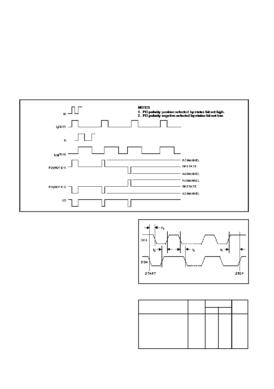
PHASE COMPARATOR
The phase comparator produces current pulses of
duration equal to the difference in phase between the
comparison frequency (fc=Rl/R), and f
VN, the divided-down
VCO frequency (Fl/N).
When status bit 4 is set high the positive polarity mode of
the output PD is selected. When fc leads f
VN the PD output
goes high; when f
VN ieads fc it goes low.
Similarly, selecting
the negative polarity mode of PD by programming bit 4 of the
status register low causes PD to have the inverse polarity. The
loop filter integrates the current pulses to produce a voltage
drive to the VCO.
No pulses are produced when locked. The lock detect
output, LD, produces a logic ‘0’ pulse equal to the phase
difference between f
C and fVN.
When the phase difference between fc and f
VN is too small
to be resolved by the phase detector then no current pulses
are produced. In this region the loop does not reduce the
close-in noise on the VCO output. This can be overcome
using a very high value resistor to leak a few nanoAmps of
current from the filter and keep the loop on the edge of the
region.
Fig. 5 Phase comparator phase diagram
PROGRAMMING
Transmission Protocol
I2C programming messages consist of an address byte
followed by a sub-address byte followed by 1, 2 or 3 bytes of
data. Bit 7 of the address byte must match the setting of the
S/D pin for the address to be recognised. This allows for
separate addressing of two NJ88C33 synthesisers on the
same bus. The sub-address should be set to select the correct
registers to be programmed and should be followed by the
appropriate number of data bytes.
Registers are not
programmed until the complete message protocol has been
checked.
Each message should commence with a START condition
and end with a STOP condition unless followed immediately
by another transfer, when the STOP condition may be omitted.
Data is transferred from the shift register to the latches on
a STOP condition or by a second START condition.
A START condition is indicated by a falling edge on the
Serial Data line, SDA, when the Serial Clock line. SCL, is high.
A rising edge on SDA when SCL is high indicates a STOP
condition as shown in Fig.6.
Data on SDA is clocked into the NJ88C33 on the rising
edge of SCL. The NJ88C33 acknowledges each byte
transferred to it by pulling the SDA line low for one cycle of SCL
after the last bit has been received.
Serial clock frequency
SCL hold after START
Data set-up time
Data hold after SCL low
SCL set-up before STOP
Symbol
Parameter
f
SCL
t
1
t
2
t
3
t
4
Unit
Min.
Max.
MHz
ns
200
20
0
20
5
I2C TIMING INFORMATION
VDD = 4.5V to 5.5V, Tamb = -40°C to +85°C
Fig. 6 I2C timing diagram
Value
相关PDF资料 |
PDF描述 |
|---|---|
| NJ903L | Silicon Junction Field-Effect Transistor |
| NJ903 | Silicon Junction Field-Effect Transistor |
| NJG1102F1 | 5015 RR 4#12 PIN PLUG |
| NJG1103F1 | MB 3C 3#20 SKT PLUG |
| NJG1103F1-C1 | 1.5/1.9GHz LOW NOISE AMPLIFIER GaAs MMIC |
相关代理商/技术参数 |
参数描述 |
|---|---|
| NJ88C33MP | 制造商:MITEL 制造商全称:Mitel Networks Corporation 功能描述:Frequency Synthesiser (I2C BUS Programmable) |
| NJ88C50 | 制造商:MITEL 制造商全称:Mitel Networks Corporation 功能描述:Dual Low Power Frequency Synthesiser |
| NJ88C50/IG/NPAS | 制造商:未知厂家 制造商全称:未知厂家 功能描述:Serial-Input Frequency Synthesizer |
| NJ88C50/MA/NP | 制造商:ZARLINK 制造商全称:Zarlink Semiconductor Inc 功能描述:Dual Low Power Frequency Synthesiser |
| NJ88C50IG | 制造商:MITEL 制造商全称:Mitel Networks Corporation 功能描述:Dual Low Power Frequency Synthesiser |
发布紧急采购,3分钟左右您将得到回复。