- 您现在的位置:买卖IC网 > PDF目录224597 > NJ88C33/MA/MP (ZARLINK SEMICONDUCTOR INC) PLL FREQUENCY SYNTHESIZER, 150 MHz, PDSO14 PDF资料下载
参数资料
| 型号: | NJ88C33/MA/MP |
| 厂商: | ZARLINK SEMICONDUCTOR INC |
| 元件分类: | PLL合成/DDS/VCOs |
| 英文描述: | PLL FREQUENCY SYNTHESIZER, 150 MHz, PDSO14 |
| 封装: | 0.150 INCH, PLASTIC, MS-012AB, SOIC-14 |
| 文件页数: | 9/15页 |
| 文件大小: | 449K |
| 代理商: | NJ88C33/MA/MP |
NJ88C33
2
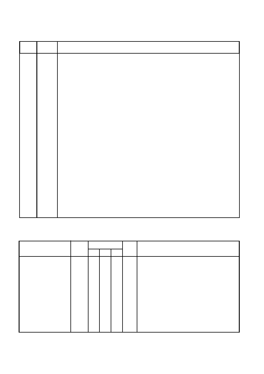
PIN DESIGNATIONS
Description
Pin
Name
V
DD
RI
S/D
SDA
SCL
PORT
MOD
FI
GND2
FVN
GND1
PD
C
LD
Pin
No.
1
2
3
4
5
6
7
8
9
10
11
12
13
14
Supply voltage (normally 5V or 3V).
Reference frequency input from an accurate source, normally a crystal oscillator. The input is normally
an AC coupled sinewave but may be a DC coupled square wave.
Single/dual modulus operating mode selection input. Single modulus operation is selected by driving
the pin low. 'High' selects dual modulus mode.
I2C bus data input pin. It is also an open-drain output for generating I2C bus acknowledge pulses.
I2C bus clock input. It can be clocked at up to 5MHz.
Output control pin, which can be programmed via the I2C bus. It can be connected to the S/D pin to
select single or dual modulus mode under bus control.
Modulus control pin. It is high in single modulus mode but switches in dual modulus operation. In dual
modulus mode, MOD remains low during operation of the A counter until A=0; MOD then remains high
until N=0, when both counters are reloaded. It can be programmed via the I2C bus as an open-drain
or push-pull output.
Frequency input from a VCO or prescaler. The input is normally an AC coupled sinewave but may be
a DC coupled square wave.
Dedicated ground for the FI input buffer. It should be connected to the VCO ground or the prescaler
ground, if used. Any noise on this pin will affect the performance of the VCO loop.
Open-drain output from the N counter.
Ground supply pin (global).
Tristate current output from the phase detector. The polarity of the output can be programmed via the
I2C bus.
Voltage doubler output. The operation of the doubler can be controlled via the I2C bus. In applications
where the voltage doubler is switched off, this pin should be connected to GND1; a reservior capacitor
should be connected from this pin to GND1 for applications where it is switched on.
Open-drain lock detect output - requires integration if used.
OPERATING RANGE
Test conditions (unless otherwise stated):
PLL locked, RI = 10MHz
Supply voltage
Ambient temperature
Supply current
Single modulus
Dual modulus
Standby mode
V
°C
mA
A
mA
V
DD
T
amb
I
DD
I
DD
I
DD
I
DD
2.5
-40
Conditions
Symbol
Min. Typ. Max.
Unit
Value
5
2.1
2
1.0
5.5
+85
3.0
1
1.5
Characteristic
FI = 50MHz, VFI = 150mVrms, N,R > 1000 without
voltage doubler, VDD = 5V, Tamb = 25°C
FI = 10MHz, VFI = 500mVrms, N,R > 1000 without
voltage doubler, VDD = 5V, Tamb = 25°C
FI = 50MHz, VFI = 150mVrms, preamp off, divider off,
VDD = 5V, Tamb = 25°C
FI = 50MHz, VFI = 150mVrms, preamp on, divider off,
VDD = 5V, Tamb = 25°C
相关PDF资料 |
PDF描述 |
|---|---|
| NJ903L | Silicon Junction Field-Effect Transistor |
| NJ903 | Silicon Junction Field-Effect Transistor |
| NJG1102F1 | 5015 RR 4#12 PIN PLUG |
| NJG1103F1 | MB 3C 3#20 SKT PLUG |
| NJG1103F1-C1 | 1.5/1.9GHz LOW NOISE AMPLIFIER GaAs MMIC |
相关代理商/技术参数 |
参数描述 |
|---|---|
| NJ88C33MP | 制造商:MITEL 制造商全称:Mitel Networks Corporation 功能描述:Frequency Synthesiser (I2C BUS Programmable) |
| NJ88C50 | 制造商:MITEL 制造商全称:Mitel Networks Corporation 功能描述:Dual Low Power Frequency Synthesiser |
| NJ88C50/IG/NPAS | 制造商:未知厂家 制造商全称:未知厂家 功能描述:Serial-Input Frequency Synthesizer |
| NJ88C50/MA/NP | 制造商:ZARLINK 制造商全称:Zarlink Semiconductor Inc 功能描述:Dual Low Power Frequency Synthesiser |
| NJ88C50IG | 制造商:MITEL 制造商全称:Mitel Networks Corporation 功能描述:Dual Low Power Frequency Synthesiser |
发布紧急采购,3分钟左右您将得到回复。