- 您现在的位置:买卖IC网 > Datasheet目录484 > NOIL1SM0300A-WWC (ON Semiconductor)IC IMAGE SENSOR LUPA300 48LLC Datasheet资料下载
参数资料
| 型号: | NOIL1SM0300A-WWC |
| 厂商: | ON Semiconductor |
| 文件页数: | 7/30页 |
| 文件大小: | 0K |
| 描述: | IC IMAGE SENSOR LUPA300 48LLC |
| 标准包装: | 1 |
| 系列: | LUPA300 |
| 象素大小: | 9.9µm x 9.9µm |
| 有源象素阵列: | 640H x 480V |
| 每秒帧数: | 250 |
| 电源电压: | 2.5 V,3.3 V |
| 类型: | CMOS 成像 |
| 封装/外壳: | 48-LCC |
| 供应商设备封装: | 48-LCC(14.22x14.22) |
| 包装: | 托盘 |
第1页第2页第3页第4页第5页第6页当前第7页第8页第9页第10页第11页第12页第13页第14页第15页第16页第17页第18页第19页第20页第21页第22页第23页第24页第25页第26页第27页第28页第29页第30页
�� �
�
�NOIL1SM0300A�
�50ns�
�CLK_ADC�
�ADC_IN�
�D1�
�D2�
�D3�
�D4�
�D5�
�D6�
�D7�
�D8�
�ADC_OUT�
�DUMMY�
�D1�
�D2�
�D3�
�D4�
�<9:0>�
�5.5� clock� cycles�
�3.7ns�
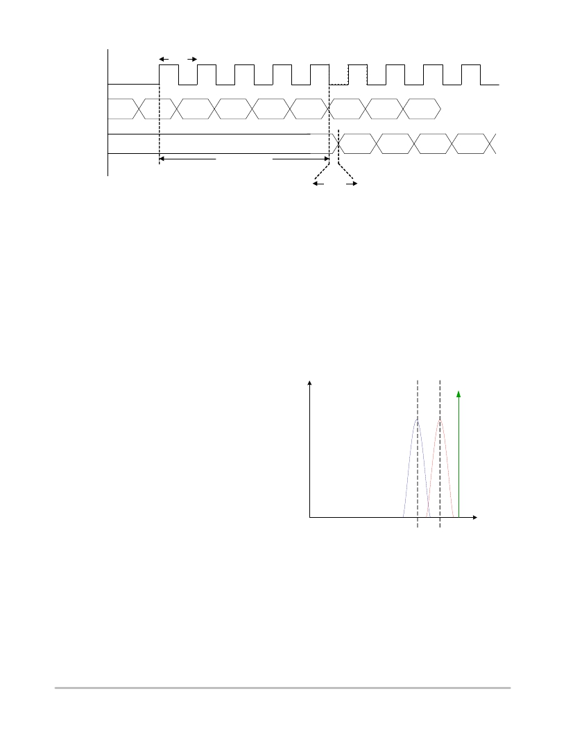
�Figure� 6.� ADC� Timing�
�Programmable� Gain� Amplifiers�
�The� programmable� gain� amplifiers� have� two� functions:�
�?� Adding� an� offset� to� the� signal� to� fit� it� into� the� range� of�
�the� ADC.� This� is� controlled� by� the� VBLACK� and�
�VOFFSET� SPI� settings.�
�?� Amplifying� the� signal� after� the� offset� is� added.�
�Offset� Regulation�
�The� purpose� of� offset� regulation� is� to� bring� the� signal� in�
�the� input� range� of� the� ADC.�
�After� the� column� amplifiers,� the� signal� from� the� pixels� has�
�a� range� from� 0.1V� (bright)� to� 1.3V� (black).� The� input� range�
�Consider� as� an� example� that� the� device� has� a� black� level� of�
�1.45V� and� a� swing� of� 100� mV.� With� this� swing,� it� fits� in� the�
�input� range� of� the� ADC,� but� a� large� part� of� the� range� of� the�
�ADC� is� not� used� in� this� case.� For� this� reason� an� offset� is�
�added� first,� to� align� the� black� level� with� the� input� range� of� the�
�ADC.� In� the� first� step,� an� offset� of� 200� mV� is� added� with� the�
�default� settings� of� VBLACK� and� VOFFSET.� This� results� in�
�the� red� histogram� with� a� average� black� level� of� 1.65V.� This�
�means� that� the� spread� on� the� black� level� falls� completely�
�inside� the� range� of� the� ADC.� In� a� second� step,� the� signal� is�
�amplified� to� use� the� full� range� of� the� ADC.�
�of� the� ADC� is� from� 0.75V� to� 1.75V.� The� amount� of� offset�
�added� is� controlled� by� two� SPI� settings:� VBLACK<7:0>� and�
�VOFFSET<7:0>.� The� formula� to� add� offset� is:�
�Voutput� =� Vsignal� +� (Voffset� -� Vblack)�
�Note� that� the� FPN� (fixed� pattern� noise)� of� the� sensor�
�causes� a� spread� of� about� 100� mV� on� the� dark� level.� To� allow�
�FPN� correction� during� post� processing� of� the� image,� this�
�spread� on� the� dark� level� needs� to� be� covered� by� the� input�
�range� of� the� ADC.� This� is� why� the� default� settings� of� the� SPI�
�are� programmed� to� add� an� offset� of� 200� mV.� This� way� the�
�dark� level� goes� from� 1.3V� to� 1.5V� and� is� the� FPN�
�information� still� converted� by� the� ADC.� To� match� the� ADC�
�range,� it� is� recommended� to� program� an� offset� of� 340� mV.� To�
�program� this� offset,� the� Voffset� and� Vblack� registers� can� be�
�1.45V�
�1.65V�
�1.75V�
�VADC_HIGH�
�used.� Figure� 7� illustrates� the� operation� of� the� offset�
�regulation� with� an� example.� The� blue� histogram� is� the�
�histogram� of� the� image� taken� after� the� column� amplifiers.�
�http://onsemi.com�
�7�
�Figure� 7.� Offset� Regulation�
�Volts�
�相关PDF资料 |
PDF描述 |
|---|---|
| NOIL2SC1300A-GDC | IC IMAGE SENSOR LUPA1300 168PGA |
| NOIV1SE025KA-GDC | IC IMAGE SENSOR 25MP 355PGA |
| NP100P04PDG-E1-AY | MOSFET P-CH -40V MP-25ZP/TO-263 |
| NP100P04PLG-E1-AY | MOSFET P-CH -40V MP-25ZP/TO-263 |
| NP100P06PDG-E1-AY | MOSFET P-CH -60V MP-25ZP/TO-263 |
相关代理商/技术参数 |
参数描述 |
|---|---|
| NOIL1SM1300AWES | 制造商:ON Semiconductor 功能描述:PW/H |
| NOIL1SM4000A | 制造商:ONSEMI 制造商全称:ON Semiconductor 功能描述:LUPA4000: 4 MegaPixel High Speed CMOS Sensor |
| NOIL1SM4000A-GDC | 功能描述:IC IMAGE SENSOR LUPA4000 127PGA RoHS:是 类别:传感器,转换器 >> 图像,相机 系列:* 标准包装:480 系列:- 象素大小:6.7µm x 6.7µm 有源象素阵列:768H x 488V 每秒帧数:52 电源电压:3.3V 类型:CMOS 成像 封装/外壳:48-QFP 供应商设备封装:48-QFP 包装:托盘 请注意:* 配用:4H2105-ND - HEADBOARD FOR KAC-004014H2104-ND - KIT EVAL FOR KAC-00401 其它名称:4H20954H2095-NDKAC-00401-CBC-LB-A0 |
| NOIL1SN3000A-GDC | 功能描述:IC IMAGE SENSOR LUPA3000 369PGA RoHS:是 类别:传感器,转换器 >> 图像,相机 系列:* 标准包装:480 系列:- 象素大小:6.7µm x 6.7µm 有源象素阵列:768H x 488V 每秒帧数:52 电源电压:3.3V 类型:CMOS 成像 封装/外壳:48-QFP 供应商设备封装:48-QFP 包装:托盘 请注意:* 配用:4H2105-ND - HEADBOARD FOR KAC-004014H2104-ND - KIT EVAL FOR KAC-00401 其它名称:4H20954H2095-NDKAC-00401-CBC-LB-A0 |
| NOIL2SC1300A-GDC | 功能描述:图像传感器和彩色传感器 LUPA1300-2 COLOR PGA168 RoHS:否 制造商:Avago Technologies 类型:Color Sensors 工作电源电压:2.5 V 封装 / 箱体: 图象大小: 颜色读出:Color 最大工作温度:+ 70 C 最小工作温度:- 25 C 封装:Reel |
发布紧急采购,3分钟左右您将得到回复。