- 您现在的位置:买卖IC网 > PDF目录18547 > NTB75N03-6G (ON Semiconductor)MOSFET N-CH 30V 75A D2PAK PDF资料下载
参数资料
| 型号: | NTB75N03-6G |
| 厂商: | ON Semiconductor |
| 文件页数: | 2/7页 |
| 文件大小: | 0K |
| 描述: | MOSFET N-CH 30V 75A D2PAK |
| 产品变化通告: | Product Discontinuation 03/Apr/2007 |
| 标准包装: | 50 |
| FET 型: | MOSFET N 通道,金属氧化物 |
| FET 特点: | 逻辑电平门 |
| 漏极至源极电压(Vdss): | 30V |
| 电流 - 连续漏极(Id) @ 25° C: | 75A |
| 开态Rds(最大)@ Id, Vgs @ 25° C: | 6.5 毫欧 @ 37.5A,10V |
| Id 时的 Vgs(th)(最大): | 2V @ 250µA |
| 闸电荷(Qg) @ Vgs: | 75nC @ 5V |
| 输入电容 (Ciss) @ Vds: | 5635pF @ 25V |
| 功率 - 最大: | 2.5W |
| 安装类型: | 表面贴装 |
| 封装/外壳: | TO-263-3,D²Pak(2 引线+接片),TO-263AB |
| 供应商设备封装: | D2PAK |
| 包装: | 管件 |
�� �
�
�NTP75N03?06,� NTB75N03?06�
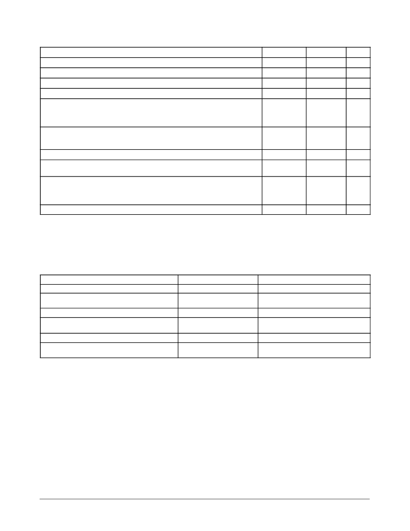
�MAXIMUM� RATINGS� (T� J� =� 25� °� C� unless� otherwise� noted)�
�Rating�
�Drain?to?Source� Voltage�
�Drain?to?Gate� Voltage� (RGS� =� 10� M� W� )�
�Gate?to?Source� Voltage� ?� Continuous�
�Non?repetitive� (tp� ≤� 10� ms)�
�Drain� Current�
�?� Continuous� @� T� C� =� 25� °� C�
�?� Continuous� @� T� C� =� 100� °� C�
�?� Single� Pulse� (tp� ≤� 10� m� s)�
�Total� Power� Dissipation� @� T� C� =� 25� °� C�
�Derate� above� 25� °� C�
�Total� Power� Dissipation� @� T� A� =� 25� °� C� (Note� 1)�
�Operating� and� Storage� Temperature� Range�
�Single� Pulse� Drain?to?Source� Avalanche� Energy� ?� Starting� T� J� =� 25� °� C�
�Symbol�
�V� DSS�
�V� DGB�
�V� GS�
�V� GS�
�I� D�
�I� D�
�I� DM�
�P� D�
�T� J� and� T� stg�
�E� AS�
�Value�
�30�
�30�
�±� 20�
�±� 24�
�75�
�59�
�225�
�125�
�1.0�
�2.5�
�?55� to� 150�
�1500�
�Unit�
�Vdc�
�Vdc�
�Vdc�
�Vdc�
�Adc�
�Apk�
�W�
�W/� °� C�
�W�
�°� C�
�mJ�
�(V� DD� =� 38� Vdc,� V� GS� =� 10� Vdc,� L� =� 1� mH,� I� L� (pk)� =� 55� A,� V� DS� =� 40� Vdc)�
�Thermal� Resistance�
�?� Junction?to?Case�
�?� Junction?to?Ambient�
�?� Junction?to?Ambient� (Note� 1)�
�Maximum� Lead� Temperature� for� Soldering� Purposes,� 1/8� in� from� case� for� 10� seconds�
�R� q� JC�
�R� q� JA�
�R� q� JA�
�T� L�
�1.0�
�62.5�
�50�
�260�
�°� C/W�
�°� C�
�Maximum� ratings� are� those� values� beyond� which� device� damage� can� occur.� Maximum� ratings� applied� to� the� device� are� individual� stress� limit�
�values� (not� normal� operating� conditions)� and� are� not� valid� simultaneously.� If� these� limits� are� exceeded,� device� functional� operation� is� not� implied,�
�damage� may� occur� and� reliability� may� be� affected.�
�1.� When� surface� mounted� to� an� FR4� board� using� the� minimum� recommended� pad� size.�
�ORDERING� INFORMATION�
�NTP75N03?06�
�NTP75N03?06G�
�NTB75N03?06�
�NTB75N03?06G�
�NTB75N03?06T4�
�NTB75N03?06T4G�
�Device�
�Package�
�TO?220�
�TO?220�
�(Pb?Free)�
�D� 2� PAK�
�D� 2� PAK�
�(Pb?Free)�
�D� 2� PAK�
�D� 2� PAK�
�Shipping� ?�
�50� Units� /� Rail�
�50� Units� /� Rail�
�50� Units� /� Rail�
�50� Units� /� Rail�
�800� Units� /� Tape� &� Reel�
�800� Units� /� Tape� &� Reel�
�(Pb?Free)�
�?For� information� on� tape� and� reel� specifications,� including� part� orientation� and� tape� sizes,� please� refer� to� our� Tape� and� Reel� Packaging�
�Specifications� Brochure,� BRD8011/D.�
�http://onsemi.com�
�2�
�相关PDF资料 |
PDF描述 |
|---|---|
| NTB75N03-006 | MOSFET N-CH 30V 75A D2PAK |
| NTB65N02RG | MOSFET N-CH 25V 7.6A D2PAK |
| NTB65N02R | MOSFET N-CH 25V 7.6A D2PAK |
| NTB60N06LG | MOSFET N-CH 60V 60A D2PAK |
| NTB60N06L | MOSFET N-CH 60V 60A D2PAK |
相关代理商/技术参数 |
参数描述 |
|---|---|
| NTB75N03-6T4G | 功能描述:MOSFET 30V 75A N-Channel RoHS:否 制造商:STMicroelectronics 晶体管极性:N-Channel 汲极/源极击穿电压:650 V 闸/源击穿电压:25 V 漏极连续电流:130 A 电阻汲极/源极 RDS(导通):0.014 Ohms 配置:Single 最大工作温度: 安装风格:Through Hole 封装 / 箱体:Max247 封装:Tube |
| NTB75N03L09 | 功能描述:MOSFET 30V 75A N-Channel RoHS:否 制造商:STMicroelectronics 晶体管极性:N-Channel 汲极/源极击穿电压:650 V 闸/源击穿电压:25 V 漏极连续电流:130 A 电阻汲极/源极 RDS(导通):0.014 Ohms 配置:Single 最大工作温度: 安装风格:Through Hole 封装 / 箱体:Max247 封装:Tube |
| NTB75N03L09G | 功能描述:MOSFET 30V 75A N-Channel RoHS:否 制造商:STMicroelectronics 晶体管极性:N-Channel 汲极/源极击穿电压:650 V 闸/源击穿电压:25 V 漏极连续电流:130 A 电阻汲极/源极 RDS(导通):0.014 Ohms 配置:Single 最大工作温度: 安装风格:Through Hole 封装 / 箱体:Max247 封装:Tube |
| NTB75N03L09G | 制造商:ON Semiconductor 功能描述:MOSFET |
| NTB75N03L09T4 | 功能描述:MOSFET 30V 75A N-Channel RoHS:否 制造商:STMicroelectronics 晶体管极性:N-Channel 汲极/源极击穿电压:650 V 闸/源击穿电压:25 V 漏极连续电流:130 A 电阻汲极/源极 RDS(导通):0.014 Ohms 配置:Single 最大工作温度: 安装风格:Through Hole 封装 / 箱体:Max247 封装:Tube |
发布紧急采购,3分钟左右您将得到回复。