- 您现在的位置:买卖IC网 > Datasheet目录488 > NTGS4141NT1G (ON Semiconductor)MOSFET N-CH 30V 3.5A 6-TSOP Datasheet资料下载
参数资料
| 型号: | NTGS4141NT1G |
| 厂商: | ON Semiconductor |
| 文件页数: | 1/6页 |
| 文件大小: | 0K |
| 描述: | MOSFET N-CH 30V 3.5A 6-TSOP |
| 产品目录绘图: | MOSFET 6-TSOP |
| 标准包装: | 10 |
| FET 型: | MOSFET N 通道,金属氧化物 |
| FET 特点: | 逻辑电平门 |
| 漏极至源极电压(Vdss): | 30V |
| 电流 - 连续漏极(Id) @ 25° C: | 3.5A |
| 开态Rds(最大)@ Id, Vgs @ 25° C: | 25 毫欧 @ 7A,10V |
| Id 时的 Vgs(th)(最大): | 3V @ 250µA |
| 闸电荷(Qg) @ Vgs: | 12nC @ 10V |
| 输入电容 (Ciss) @ Vds: | 560pF @ 24V |
| 功率 - 最大: | 500mW |
| 安装类型: | 表面贴装 |
| 封装/外壳: | SC-74,SOT-457 |
| 供应商设备封装: | 6-TSOP |
| 包装: | 标准包装 |
| 产品目录页面: | 1558 (CN2011-ZH PDF) |
| 其它名称: | NTGS4141NT1GOSDKR |
�� �
�
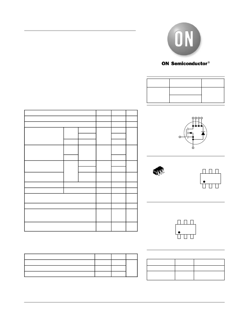
�NTGS4141N�
�Power� MOSFET�
�30� V,� 7.0� A,� Single� N� ?� Channel,� TSOP� ?� 6�
�Features�
�?� Low� R� DS(on)�
�?� Low� Gate� Charge�
�?� Pb� ?� Free� Package� is� Available�
�http://onsemi.com�
�Applications�
�?� Load� Switch�
�?� Notebook� PC�
�?� Desktop� PC�
�V� (BR)DSS�
�30� V�
�R� DS(on)� TYP�
�21.5� m� W� @� 10� V�
�30� m� W� @� 4.5� V�
�I� D� MAX�
�7.0� A�
�MAXIMUM� RATINGS� (T� J� =� 25� °� C� unless� otherwise� noted)�
�Rating� Symbol�
�Drain� ?� to� ?� Source� Voltage� V� DSS�
�Value�
�30�
�Unit�
�V�
�N� ?� Channel�
�Drain� 1� 2� 5� 6�
�Gate� ?� to� ?� Source� Voltage�
�V� GS�
�±� 20�
�V�
�Continuous� Drain�
�Current� (Note� 1)�
�Steady�
�State�
�T� A� =� 25� °� C�
�T� A� =� 85� °� C�
�I� D�
�5.0�
�3.6�
�A�
�Gate� 3�
�t� ≤� 10� s�
�T� A� =� 25� °� C�
�7.0�
�Power� Dissipation�
�(Note� 1)�
�Steady�
�State�
�T� A� =� 25� °� C�
�P� D�
�1.0�
�W�
�Source� 4�
�1�
�Continuous� Drain�
�Current� (Note� 2)�
�Power� Dissipation�
�(Note� 2)�
�Pulsed� Drain� Current�
�t� ≤� 10� s�
�Steady� T� A� =� 25� °� C�
�State�
�T� A� =� 85� °� C�
�T� A� =� 25� °� C�
�t� p� =� 10� m� s,� V� GS� =10V�
�I� D�
�P� D�
�I� DM�
�2.0�
�3.5�
�2.5�
�0.5�
�45�
�A�
�W�
�A�
�TSOP� ?� 6�
�CASE� 318G�
�STYLE� 1�
�S4� =� Device� Code�
�MARKING�
�DIAGRAM�
�S4� M� G�
�G�
�Pulsed� Drain� Current� t� p� =� 30� m� s,� V� GS� =5V�
�Operating� Junction� and� Storage� Temperature�
�Source� Current� (Body� Diode)�
�Single� Pulse� Drain� ?� to� ?� Source� Avalanche� Energy�
�(V� DD� =� 30� V,� I� L� =� 10.4� A,� V� GS� =� 10� V,�
�L� =� 1.0� mH,� R� G� =� 25� W� )�
�Lead� Temperature� for� Soldering� Purposes�
�(1/8� ″� from� case� for� 10� s)�
�I� D�
�T� J� ,�
�T� STG�
�I� S�
�EAS�
�T� L�
�30�
�?� 55� to�
�150�
�2.0�
�54�
�260�
�A�
�°� C�
�A�
�mJ�
�°� C�
�M� =� Date� Code�
�G� =� Pb� ?� Free� Package�
�(Note:� Microdot� may� be� in� either� location)�
�PIN� ASSIGNMENT�
�Drain� Drain� Source�
�6� 5� 4�
�Stresses� exceeding� Maximum� Ratings� may� damage� the� device.� Maximum�
�Ratings� are� stress� ratings� only.� Functional� operation� above� the� Recommended�
�Operating� Conditions� is� not� implied.� Extended� exposure� to� stresses� above� the�
�Recommended� Operating� Conditions� may� affect� device� reliability.�
�THERMAL� RESISTANCE� RATINGS�
�1� 2� 3�
�Drain� Drain� Gate�
�Rating�
�Symbol�
�Max�
�Unit�
�ORDERING� INFORMATION�
�Junction� ?� to� ?� Ambient� –� Steady� State� (Note� 1)�
�Junction� ?� to� ?� Ambient� –� t� ≤� 10� s� (Note� 1)�
�R� θ� JA�
�R� θ� JA�
�125�
�62.5�
�°� C/W�
�Device�
�NTGS4141NT1�
�Package�
�TSOP� ?� 6�
�Shipping� ?�
�3000/Tape� &� Reel�
�3000/Tape� &� Reel�
�NTGS4141NT1G�
�Junction� ?� to� ?� Ambient� –� Steady� State� (Note� 2)� R� θ� JA� 248�
�1.� Surface� ?� mounted� on� FR4� board� using� 1� inch� sq� pad� size�
�(Cu� area� =� 1.127� in� sq� [1� oz]� including� traces).�
�2.� Surface� ?� mounted� on� FR4� board� using� the� minimum� recommended� pad� size�
�(Cu� area� =� 0.0773� in� sq).�
�TSOP� ?� 6�
�(Pb� ?� Free)�
�?For� information� on� tape� and� reel� specifications,�
�including� part� orientation� and� tape� sizes,� please�
�refer� to� our� Tape� and� Reel� Packaging� Specification�
�Brochure,� BRD8011/D.�
�?� Semiconductor� Components� Industries,� LLC,� 2012�
�April,� 2012� ?� Rev.� 5�
�1�
�Publication� Order� Number:�
�NTGS4141N/D�
�相关PDF资料 |
PDF描述 |
|---|---|
| NTGS5120PT1G | MOSFET P-CH 60V 1.8A 6-TSOP |
| NTHC5513T1 | MOSFET N/P-CH 20V 2.1A CHIPFET |
| NTHD2102PT1G | MOSFET PWR P-CH DUAL 8V CHIPFET |
| NTHD2110TT1G | MOSFET P-CH 12V 4.5A CHIPFET |
| NTHD3100CT3G | MOSFET N/P-CH COMPL 20V CHIPFET |
相关代理商/技术参数 |
参数描述 |
|---|---|
| NTGS4141NT1G-CUT TAPE | 制造商:ON 功能描述:NTGS Series N-Channel 30 V 21.5 mOhm 1 W Surface Mount Power MOSFET - TSOP-6 |
| NTGS5120P | 制造商:ONSEMI 制造商全称:ON Semiconductor 功能描述:Power MOSFET −60 V, −2.9 A, Single P−Channel, TSOP−6 |
| NTGS5120PT1G | 功能描述:MOSFET PFET TSOP6 60V 2.5A 110mOhm RoHS:否 制造商:STMicroelectronics 晶体管极性:N-Channel 汲极/源极击穿电压:650 V 闸/源击穿电压:25 V 漏极连续电流:130 A 电阻汲极/源极 RDS(导通):0.014 Ohms 配置:Single 最大工作温度: 安装风格:Through Hole 封装 / 箱体:Max247 封装:Tube |
| NTGW | 功能描述:烙铁 Weller Cylind Tip For WMP Solder Penc RoHS:否 制造商:Weller 产品:Soldering Stations 类型:Digital, Iron, Stand, Cleaner 瓦特:50 W 最大温度:+ 850 F 电缆类型:US Cord Included |
| NTH | 功能描述:烙铁 Weller Chisel Tip For WMP Solder Penc RoHS:否 制造商:Weller 产品:Soldering Stations 类型:Digital, Iron, Stand, Cleaner 瓦特:50 W 最大温度:+ 850 F 电缆类型:US Cord Included |
发布紧急采购,3分钟左右您将得到回复。