- 您现在的位置:买卖IC网 > Datasheet目录489 > NTHD2110TT1G (ON Semiconductor)MOSFET P-CH 12V 4.5A CHIPFET Datasheet资料下载
参数资料
| 型号: | NTHD2110TT1G |
| 厂商: | ON Semiconductor |
| 文件页数: | 1/7页 |
| 文件大小: | 0K |
| 描述: | MOSFET P-CH 12V 4.5A CHIPFET |
| 产品变化通告: | Product Obsolescence 19/Dec/2008 |
| 标准包装: | 3,000 |
| FET 型: | MOSFET P 通道,金属氧化物 |
| FET 特点: | 逻辑电平门 |
| 漏极至源极电压(Vdss): | 12V |
| 电流 - 连续漏极(Id) @ 25° C: | 4.5A |
| 开态Rds(最大)@ Id, Vgs @ 25° C: | 40 毫欧 @ 6.4A,4.5V |
| Id 时的 Vgs(th)(最大): | 850mV @ 250µA |
| 闸电荷(Qg) @ Vgs: | 14nC @ 4.5V |
| 输入电容 (Ciss) @ Vds: | 1072pF @ 6V |
| 功率 - 最大: | 1.1W |
| 安装类型: | 表面贴装 |
| 封装/外壳: | 8-SMD,扁平引线 |
| 供应商设备封装: | ChipFET? |
| 包装: | 带卷 (TR) |
��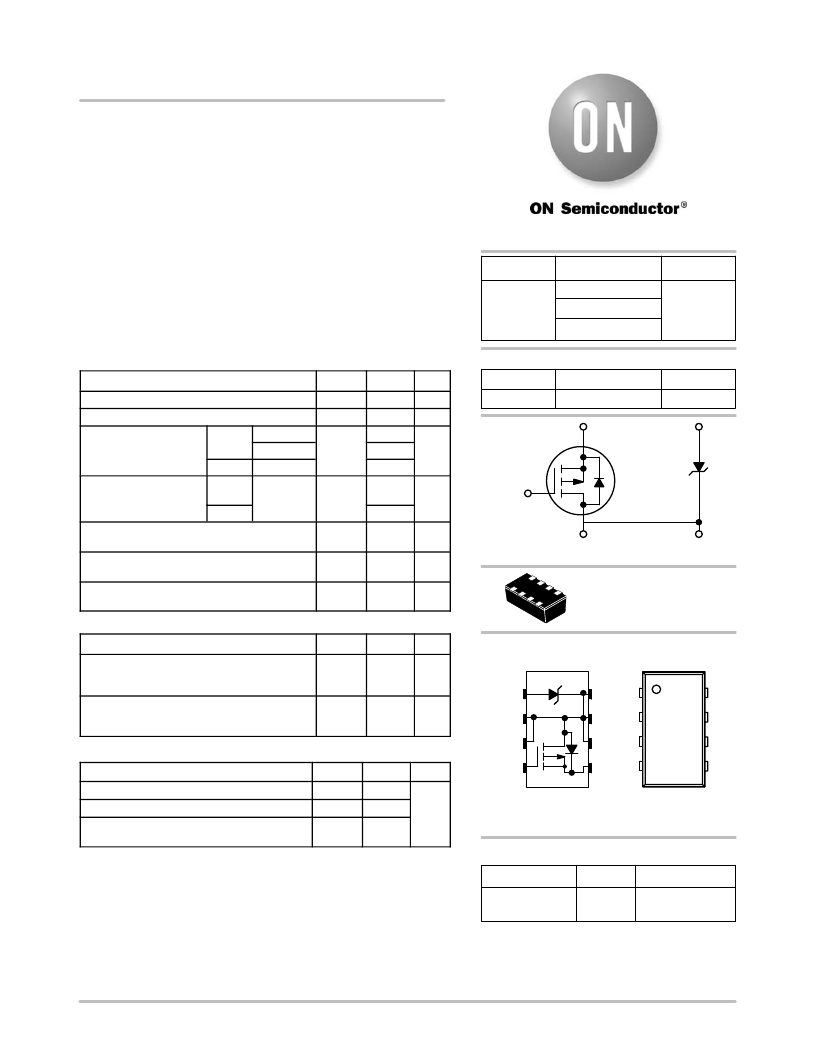 �
�
�NTHD2110T�
�Power� MOSFET�
�-12� V,� -6.4� A,� Single� P-Channel� +TVS,�
�ChipFET� t� Package�
�Features�
�?� Low� R� DS(on)� MOSFET� and� TVS� Diode� ChipFET� Package�
�?� Integrated� Drain� Side� TVS� for� 15� kV� Contact� Discharge� ESD�
�Protection�
�http://onsemi.com�
�AND� PIN� A�
�?�
�?�
�1.8� V� Gate� Rating�
�This� is� a� Pb-Free� Device�
�V� (BR)DSS�
�R� DS(on)� MAX�
�40� m� W� @� -4.5� V�
�I� D� MAX�
�Applications�
�?� Battery� Switch� and� Load� Management� Applications� in� Portable�
�Equipment�
�MOSFET� MAXIMUM� RATINGS� (T� J� =� 25� °� C� unless� otherwise� noted)�
�-12� V�
�53� m� W� @� -2.5� V�
�80� m� W� @� -1.8� V�
�TVS�
�-6.4� A�
�Parameter�
�Drain-to-Source� Voltage�
�Symbol�
�V� DSS�
�Value�
�-12�
�Unit�
�V�
�V� RWM�
�12�
�V� C� @� MAX� I� PP�
�21.5�
�I� PP� MAX�
�6.2� A�
�Gate-to-Source� Voltage�
�Continuous� Drain�
�Current� (Note� 1)�
�Steady�
�State�
�T� A� =� 25� °� C�
�T� A� =� 85� °� C�
�V� GS�
�I� D�
�"� 8�
�-4.5�
�-3.2�
�V�
�A�
�S�
�A�
�t� ≤� 5s�
�T� A� =� 25� °� C�
�-6.4�
�Power� Dissipation�
�(Note� 1)�
�Steady�
�State�
�T� A� =� 25� °� C�
�P� D�
�1.1�
�W�
�G�
�t� ≤� 5s�
�2.3�
�Operating� Junction� and� Storage� Temperature�
�Storage� Temperature� Range�
�T� J� ,�
�T� STG�
�TJ�
�-55� to�
�150�
�-55� to�
�°� C�
�°� C�
�D�
�P-Channel� MOSFET�
�C�
�TVS� Diode�
�150�
�Lead� Temperature� for� Soldering� Purposes�
�(1/8� ″� from� case� for� 10� seconds)�
�T� L�
�260�
�°� C�
�8�
�ChipFET�
�CASE� 1206A�
�TVS� MAXIMUM� RATINGS� (T� J� =� 25� °� C� unless� otherwise� noted)�
�1�
�STYLE� 6�
�Parameter�
�Peak� Power� Dissipation�
�Symbol�
�PPK�
�Value�
�150�
�Unit�
�W�
�PIN�
�CONNECTIONS�
�MARKING�
�DIAGRAM�
�8� x� 20� ms� Double� Exponential� Waveform�
�(Note� 2)�
�Human� Body� Model� (HBM)�
�Machine� Model� (MM)�
�IEC� 61000-4-2� Specification� (Contact)�
�ESD�
�16�
�400�
�30�
�kV�
�V�
�kV�
�A�
�D�
�1�
�2�
�8�
�7�
�6�
�C/D�
�D�
�1�
�2�
�8�
�7�
�THERMAL� RESISTANCE� RATINGS�
�D�
�3�
�D�
�3�
�6�
�Parameter�
�Symbol�
�Max�
�Unit�
�G�
�4�
�5�
�S�
�4�
�5�
�Junction-to-Ambient� –� Steady� State� (Note� 1)�
�Junction-to-Ambient� –� t� ≤� 5� s� (Note� 1)�
�Junction-to-Ambient� -� Steady� State� Min� Pad�
�(Note� 3)�
�R� q� JA�
�R� q� JA�
�R� q� JA�
�110�
�55�
�225�
�°� C/W�
�FTZ�
�M�
�G�
�=� Specific� Device� Code�
�=� Month� Code�
�=� Pb-Free� Package�
�Stresses� exceeding� Maximum� Ratings� may� damage� the� device.� Maximum�
�Ratings� are� stress� ratings� only.� Functional� operation� above� the� Recommended�
�ORDERING� INFORMATION�
�Operating� Conditions� is� not� implied.� Extended� exposure� to� stresses� above� the�
�Recommended� Operating� Conditions� may� affect� device� reliability.�
�1.� Surface-mounted� on� FR4� board� using� 1� in� sq� pad� size� (Cu� area� =� 1.127� in� sq�
�Device�
�NTHD2110TT1G�
�Package�
�ChipFET�
�Shipping� ?�
�3000/Tape� &� Reel�
�[1� oz]� including� traces).�
�2.� Nonrepetitive� Current� Pulse� per� Figure� 11.�
�3.� Surface� Mounted� on� FR4� board� using� 1� in� sq� size� (Cu� area� =� 1.127� in� sq�
�[1� oz]� included� traces).�
�(Pb-Free)�
�?For� information� on� tape� and� reel� specifications,�
�including� part� orientation� and� tape� sizes,� please�
�refer� to� our� Tape� and� Reel� Packaging� Specifications�
�Brochure,� BRD8011/D.�
�?� Semiconductor� Components� Industries,� LLC,� 2008�
�March,� 2008� -� Rev.� 0�
�1�
�Publication� Order� Number:�
�NTHD2110T� /� D�
�相关PDF资料 |
PDF描述 |
|---|---|
| NTHD3100CT3G | MOSFET N/P-CH COMPL 20V CHIPFET |
| NTHD3101FT3G | MOSFET P-CH 20V 3.2A CHIPFET |
| NTHD3102CT1G | MOSFET N/P-CH COMPL 20V CHIPFET |
| NTHD3133PFT3G | MOSFET P-CH SGL 20V CHIPFET |
| NTHD4102PT3G | MOSFET P-CH DUAL 20V CHIPFET |
相关代理商/技术参数 |
参数描述 |
|---|---|
| NTHD3100C | 制造商:ONSEMI 制造商全称:ON Semiconductor 功能描述:Power MOSFET 20 V, +3.9 A /−4.4 A, Complementary ChipFET |
| NTHD3100CT1 | 功能描述:MOSFET 20V +3.9A/-4.4A RoHS:否 制造商:STMicroelectronics 晶体管极性:N-Channel 汲极/源极击穿电压:650 V 闸/源击穿电压:25 V 漏极连续电流:130 A 电阻汲极/源极 RDS(导通):0.014 Ohms 配置:Single 最大工作温度: 安装风格:Through Hole 封装 / 箱体:Max247 封装:Tube |
| NTHD3100CT1G | 功能描述:MOSFET 20V +3.9A/-4.4A Complementary RoHS:否 制造商:STMicroelectronics 晶体管极性:N-Channel 汲极/源极击穿电压:650 V 闸/源击穿电压:25 V 漏极连续电流:130 A 电阻汲极/源极 RDS(导通):0.014 Ohms 配置:Single 最大工作温度: 安装风格:Through Hole 封装 / 箱体:Max247 封装:Tube |
| NTHD3100CT3 | 功能描述:MOSFET 20V +3.9A/-4.4A RoHS:否 制造商:STMicroelectronics 晶体管极性:N-Channel 汲极/源极击穿电压:650 V 闸/源击穿电压:25 V 漏极连续电流:130 A 电阻汲极/源极 RDS(导通):0.014 Ohms 配置:Single 最大工作温度: 安装风格:Through Hole 封装 / 箱体:Max247 封装:Tube |
| NTHD3100CT3G | 功能描述:MOSFET 20V +3.9A/-4.4A Complementary RoHS:否 制造商:STMicroelectronics 晶体管极性:N-Channel 汲极/源极击穿电压:650 V 闸/源击穿电压:25 V 漏极连续电流:130 A 电阻汲极/源极 RDS(导通):0.014 Ohms 配置:Single 最大工作温度: 安装风格:Through Hole 封装 / 箱体:Max247 封装:Tube |
发布紧急采购,3分钟左右您将得到回复。