- 您现在的位置:买卖IC网 > Datasheet目录489 > NTHD2102PT1G (ON Semiconductor)MOSFET PWR P-CH DUAL 8V CHIPFET Datasheet资料下载
参数资料
| 型号: | NTHD2102PT1G |
| 厂商: | ON Semiconductor |
| 文件页数: | 6/6页 |
| 文件大小: | 0K |
| 描述: | MOSFET PWR P-CH DUAL 8V CHIPFET |
| 产品变化通告: | Product Obsolescence 24/Jan/2011 |
| 标准包装: | 1 |
| FET 型: | 2 个 P 沟道(双) |
| FET 特点: | 逻辑电平门 |
| 漏极至源极电压(Vdss): | 8V |
| 电流 - 连续漏极(Id) @ 25° C: | 3.4A |
| 开态Rds(最大)@ Id, Vgs @ 25° C: | 58 毫欧 @ 3.4A,4.5V |
| Id 时的 Vgs(th)(最大): | 1.5V @ 250µA |
| 闸电荷(Qg) @ Vgs: | 16nC @ 2.5V |
| 输入电容 (Ciss) @ Vds: | 715pF @ 6.4V |
| 功率 - 最大: | 1.1W |
| 安装类型: | 表面贴装 |
| 封装/外壳: | 8-SMD,扁平引线 |
| 供应商设备封装: | ChipFET? |
| 包装: | 剪切带 (CT) |
| 其它名称: | NTHD2102PT1GOSCT |
�� �
�
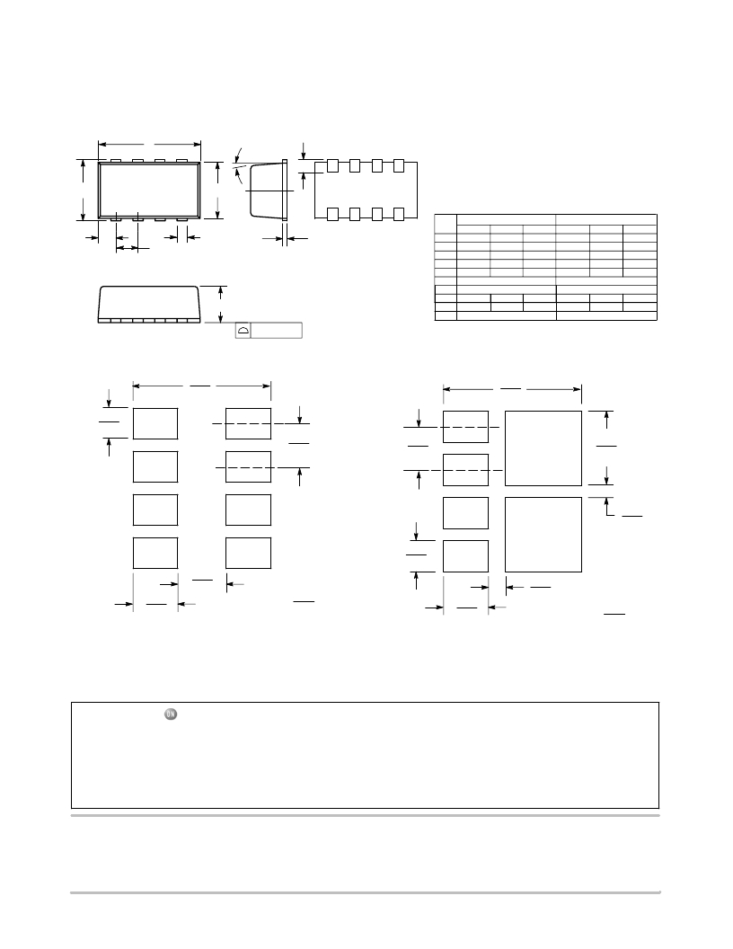
�NTHD2102P�
�PACKAGE� DIMENSIONS�
�ChipFET� ]�
�CASE� 1206A?03�
�ISSUE� G�
�D�
�q�
�NOTES:�
�1.� DIMENSIONING� AND� TOLERANCING� PER� ANSI� Y14.5M,� 1982.�
�H� E�
�8�
�1�
�7�
�2�
�6�
�3�
�5�
�4�
�E�
�L�
�5�
�4�
�6�
�3�
�7�
�2�
�8�
�1�
�2.� CONTROLLING� DIMENSION:� MILLIMETER.�
�3.� MOLD� GATE� BURRS� SHALL� NOT� EXCEED� 0.13� MM� PER� SIDE.�
�4.� LEADFRAME� TO� MOLDED� BODY� OFFSET� IN� HORIZONTAL�
�AND� VERTICAL� SHALL� NOT� EXCEED� 0.08� MM.�
�5.� DIMENSIONS� A� AND� B� EXCLUSIVE� OF� MOLD� GATE� BURRS.�
�6.� NO� MOLD� FLASH� ALLOWED� ON� THE� TOP� AND� BOTTOM� LEAD�
�SURFACE.�
�MILLIMETERS�
�INCHES�
�DIM�
�MIN�
�NOM� MAX�
�MIN�
�NOM�
�MAX�
�e1�
�b�
�c�
�A�
�1.00�
�1.05� 1.10�
�0.039�
�0.041�
�0.043�
�e�
�A�
�STYLE� 2:�
�PIN� 1.�
�2.�
�3.�
�4.�
�5.�
�6.�
�7.�
�8.�
�SOURCE� 1�
�GATE� 1�
�SOURCE� 2�
�GATE� 2�
�DRAIN� 2�
�DRAIN� 2�
�DRAIN� 1�
�DRAIN� 1�
�b�
�c�
�D�
�E�
�e�
�e1�
�L�
�H� E�
�q�
�0.25� 0.30� 0.35�
�0.10� 0.15� 0.20�
�2.95� 3.05� 3.10�
�1.55� 1.65� 1.70�
�0.65� BSC�
�0.55� BSC�
�0.28� 0.35� 0.42�
�1.80� 1.90� 2.00�
�5� °� NOM�
�0.010�
�0.004�
�0.116�
�0.061�
�0.011�
�0.071�
�0.012�
�0.006�
�0.120�
�0.065�
�0.025� BSC�
�0.022� BSC�
�0.014�
�0.075�
�5� °� NOM�
�0.014�
�0.008�
�0.122�
�0.067�
�0.017�
�0.079�
�0.05� (0.002)�
�SOLDERING� FOOTPRINT*�
�0� .45� 7�
�0.018�
�2� .03� 2�
�0.08�
�2� .03� 2�
�0.08�
�0.63� 5�
�0.025�
�0� .63� 5�
�0.025�
�1� .09� 2�
�0.043�
�0.17� 8�
�0.007�
�0.45� 7�
�0.018�
�0.66�
�0.026�
�0.711�
�0.028�
�SCALE� 20:1�
�mm�
�inches�
�0.66�
�0.026�
�0� .25� 4�
�0.010�
�SCALE� 20:1�
�mm�
�inches�
�Basic�
�Style� 2�
�*For� additional� information� on� our� Pb?Free� strategy� and� soldering�
�details,� please� download� the� ON� Semiconductor� Soldering� and�
�Mounting� Techniques� Reference� Manual,� SOLDERRM/D.�
�ChipFET� is� a� trademark� of� Vishay� Siliconix.�
�ON� Semiconductor� and� are� registered� trademarks� of� Semiconductor� Components� Industries,� LLC� (SCILLC).� SCILLC� reserves� the� right� to� make� changes� without� further� notice�
�to� any� products� herein.� SCILLC� makes� no� warranty,� representation� or� guarantee� regarding� the� suitability� of� its� products� for� any� particular� purpose,� nor� does� SCILLC� assume� any� liability�
�arising� out� of� the� application� or� use� of� any� product� or� circuit,� and� specifically� disclaims� any� and� all� liability,� including� without� limitation� special,� consequential� or� incidental� damages.�
�“Typical”� parameters� which� may� be� provided� in� SCILLC� data� sheets� and/or� specifications� can� and� do� vary� in� different� applications� and� actual� performance� may� vary� over� time.� All�
�operating� parameters,� including� “Typicals”� must� be� validated� for� each� customer� application� by� customer’s� technical� experts.� SCILLC� does� not� convey� any� license� under� its� patent� rights�
�nor� the� rights� of� others.� SCILLC� products� are� not� designed,� intended,� or� authorized� for� use� as� components� in� systems� intended� for� surgical� implant� into� the� body,� or� other� applications�
�intended� to� support� or� sustain� life,� or� for� any� other� application� in� which� the� failure� of� the� SCILLC� product� could� create� a� situation� where� personal� injury� or� death� may� occur.� Should�
�Buyer� purchase� or� use� SCILLC� products� for� any� such� unintended� or� unauthorized� application,� Buyer� shall� indemnify� and� hold� SCILLC� and� its� officers,� employees,� subsidiaries,� affiliates,�
�and� distributors� harmless� against� all� claims,� costs,� damages,� and� expenses,� and� reasonable� attorney� fees� arising� out� of,� directly� or� indirectly,� any� claim� of� personal� injury� or� death�
�associated� with� such� unintended� or� unauthorized� use,� even� if� such� claim� alleges� that� SCILLC� was� negligent� regarding� the� design� or� manufacture� of� the� part.� SCILLC� is� an� Equal�
�Opportunity/Affirmative� Action� Employer.� This� literature� is� subject� to� all� applicable� copyright� laws� and� is� not� for� resale� in� any� manner.�
�PUBLICATION� ORDERING� INFORMATION�
�LITERATURE� FULFILLMENT� :�
�N.� American� Technical� Support� :� 800?282?9855� Toll� Free�
�ON� Semiconductor� Website� :� http://onsemi.com�
�Literature� Distribution� Center� for� ON� Semiconductor�
�P.O.� Box� 61312,� Phoenix,� Arizona� 85082?1312� USA�
�USA/Canada�
�Order� Literature� :� http://www.onsemi.com/litorder�
�Fax� :� 480?829?7709� or� 800?344?3867� Toll� Free� USA/Canada�
�Phone� :� 480?829?7710� or� 800?344?3860� Toll� Free� USA/Canada� Japan� :� ON� Semiconductor,� Japan� Customer� Focus� Center�
�2?9?1� Kamimeguro,� Meguro?ku,� Tokyo,� Japan� 153?0051�
�Email� :� orderlit@onsemi.com� Phone� :� 81?3?5773?3850�
�http://onsemi.com�
�6�
�For� additional� information,� please� contact� your�
�local� Sales� Representative.�
�NTHD2102P/D�
�相关PDF资料 |
PDF描述 |
|---|---|
| NTHD2110TT1G | MOSFET P-CH 12V 4.5A CHIPFET |
| NTHD3100CT3G | MOSFET N/P-CH COMPL 20V CHIPFET |
| NTHD3101FT3G | MOSFET P-CH 20V 3.2A CHIPFET |
| NTHD3102CT1G | MOSFET N/P-CH COMPL 20V CHIPFET |
| NTHD3133PFT3G | MOSFET P-CH SGL 20V CHIPFET |
相关代理商/技术参数 |
参数描述 |
|---|---|
| NTHD2110T | 制造商:ONSEMI 制造商全称:ON Semiconductor 功能描述:Power MOSFET -12 V, -6.4 A, Single P-Channel +TVS, ChipFET? Package |
| NTHD2110TT1G | 功能描述:MOSFET P-CH 12V 4.5A CHIPFET RoHS:是 类别:分离式半导体产品 >> FET - 单 系列:- 标准包装:1,000 系列:MESH OVERLAY™ FET 型:MOSFET N 通道,金属氧化物 FET 特点:逻辑电平门 漏极至源极电压(Vdss):200V 电流 - 连续漏极(Id) @ 25° C:18A 开态Rds(最大)@ Id, Vgs @ 25° C:180 毫欧 @ 9A,10V Id 时的 Vgs(th)(最大):4V @ 250µA 闸电荷(Qg) @ Vgs:72nC @ 10V 输入电容 (Ciss) @ Vds:1560pF @ 25V 功率 - 最大:40W 安装类型:通孔 封装/外壳:TO-220-3 整包 供应商设备封装:TO-220FP 包装:管件 |
| NTHD3100C | 制造商:ONSEMI 制造商全称:ON Semiconductor 功能描述:Power MOSFET 20 V, +3.9 A /−4.4 A, Complementary ChipFET |
| NTHD3100CT1 | 功能描述:MOSFET 20V +3.9A/-4.4A RoHS:否 制造商:STMicroelectronics 晶体管极性:N-Channel 汲极/源极击穿电压:650 V 闸/源击穿电压:25 V 漏极连续电流:130 A 电阻汲极/源极 RDS(导通):0.014 Ohms 配置:Single 最大工作温度: 安装风格:Through Hole 封装 / 箱体:Max247 封装:Tube |
| NTHD3100CT1G | 功能描述:MOSFET 20V +3.9A/-4.4A Complementary RoHS:否 制造商:STMicroelectronics 晶体管极性:N-Channel 汲极/源极击穿电压:650 V 闸/源击穿电压:25 V 漏极连续电流:130 A 电阻汲极/源极 RDS(导通):0.014 Ohms 配置:Single 最大工作温度: 安装风格:Through Hole 封装 / 箱体:Max247 封装:Tube |
发布紧急采购,3分钟左右您将得到回复。