- 您现在的位置:买卖IC网 > Datasheet目录489 > NTJD1155LT1 (ON Semiconductor)MOSFET/LOAD SWITCH HI 8V SOT-363 Datasheet资料下载
参数资料
| 型号: | NTJD1155LT1 |
| 厂商: | ON Semiconductor |
| 文件页数: | 1/5页 |
| 文件大小: | 0K |
| 描述: | MOSFET/LOAD SWITCH HI 8V SOT-363 |
| 产品变化通告: | Product Discontinuation 20/Aug/2008 |
| 标准包装: | 3,000 |
| FET 型: | N 和 P 沟道 |
| FET 特点: | 标准 |
| 漏极至源极电压(Vdss): | 8V |
| 电流 - 连续漏极(Id) @ 25° C: | 1.3A |
| 开态Rds(最大)@ Id, Vgs @ 25° C: | 175 毫欧 @ 1.2A,4.5V |
| Id 时的 Vgs(th)(最大): | 1V @ 250µA |
| 功率 - 最大: | 400mW |
| 安装类型: | 表面贴装 |
| 封装/外壳: | 6-TSSOP,SC-88,SOT-363 |
| 供应商设备封装: | SOT-363 |
| 包装: | 带卷 (TR) |
�� �
�
�NTJD1155L�
�Power� MOSFET�
�8� V,� +� 1.3� A,� High� Side� Load� Switch� with�
�Level� ?� Shift,� P� ?� Channel� SC� ?� 88�
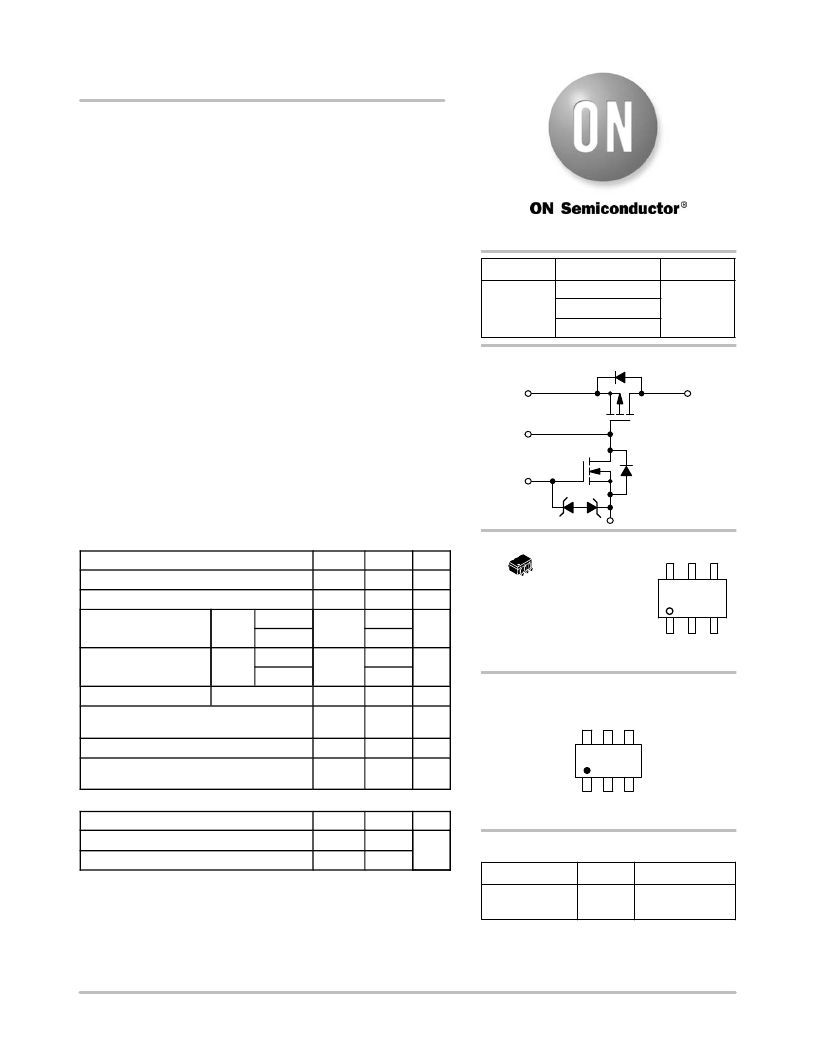
�The� NTJD1155L� integrates� a� P� and� N� ?� Channel� MOSFET� in� a� single�
�package.� This� device� is� particularly� suited� for� portable� electronic�
�equipment� where� low� control� signals,� low� battery� voltages� and� high�
�http://onsemi.com�
�load� currents� are� needed.� The� P� ?� Channel� device� is� specifically�
�designed� as� a� load� switch� using� ON� Semiconductor� state� ?� of� ?� the� ?� art�
�trench� technology.� The� N� ?� Channel,� with� an� external� resistor� (R1),�
�functions� as� a� level� ?� shift� to� drive� the� P� ?� Channel.� The� N� ?� Channel�
�MOSFET� has� internal� ESD� protection� and� can� be� driven� by� logic�
�signals� as� low� as� 1.5� V.� The� NTJD1155L� operates� on� supply� lines� from�
�V� (BR)DSS�
�8.0� V�
�R� DS(on)� TYP�
�130� m� W� @� ?� 4.5� V�
�170� m� W� @� ?� 2.5� V�
�260� m� W� @� ?� 1.8� V�
�I� D� MAX�
�±� 1.3� A�
�1.8� to� 8.0� V� and� can� drive� loads� up� to� 1.3� A� with� 8.0� V� applied� to� both�
�V� IN� and� V� ON/OFF.�
�SIMPLIFIED� SCHEMATIC�
�Features�
�?� Extremely� Low� R� DS(on)� P� ?� Channel� Load� Switch� MOSFET�
�?� Level� Shift� MOSFET� is� ESD� Protected�
�?� Low� Profile,� Small� Footprint� Package�
�?� V� IN� Range� 1.8� to� 8.0� V�
�?� ON/OFF� Range� 1.5� to� 8.0� V�
�?� These� Devices� are� Pb� ?� Free� and� are� RoHS� Compliant�
�4�
�6�
�5�
�1�
�Q2�
�Q1�
�2,3�
�T� A� =� 85� °� C�
�T� A� =� 85� °� C�
�1�
�MAXIMUM� RATINGS� (T� J� =� 25� °� C� unless� otherwise� noted)�
�Rating� Symbol�
�Input� Voltage� (V� DSS� ,� P� ?� Ch)� V� IN�
�ON/OFF� Voltage� (V� GS� ,� N� ?� Ch)� V� ON/OFF�
�Continuous� Load� Current� Steady� T� A� =� 25� °� C� I� L�
�(Note� 1)� State�
�Power� Dissipation� Steady� T� A� =� 25� °� C� P� D�
�(Note� 1)� State�
�Pulsed� Load� Current� t� p� =� 10� m� s� I� LM�
�Value�
�8.0�
�8.0�
�±� 1.3�
�±� 0.9�
�0.40�
�0.20�
�±� 3.9�
�Unit�
�V�
�V�
�A�
�W�
�A�
�MARKING�
�SC� ?� 88� DIAGRAM�
�(SOT� ?� 363)�
�CASE� 419B�
�STYLE� 30� TB� M� G�
�G�
�TB� =� Device� Code�
�M� =� Date� Code� 1�
�G� =� Pb� ?� Free� Package�
�(Note:� Microdot� may� be� in� either� location)�
�PIN� ASSIGNMENT�
�Operating� Junction� and� Storage� Temperature�
�T� J� ,�
�T� STG�
�?� 55� to�
�150�
�°� C�
�D1/G2�
�6�
�G1�
�5�
�S2�
�4�
�Source� Current� (Body� Diode)�
�Lead� Temperature� for� Soldering� Purposes�
�(1/8� ″� from� case� for� 10� s)�
�I� S�
�T� L�
�?� 0.4�
�260�
�A�
�°� C�
�THERMAL� CHARACTERISTICS�
�Characteristic�
�Symbol�
�Max�
�Unit�
�1�
�S1�
�2� 3�
�D2� D2�
�Junction� ?� to� ?� Ambient� –� Steady� State� (Note� 1)� R� q� JA� 320� °� C/W�
�Junction� ?� to� ?� Foot� –� Steady� State� (Note� 1)� R� q� JF� 220�
�Stresses� exceeding� Maximum� Ratings� may� damage� the� device.� Maximum�
�Ratings� are� stress� ratings� only.� Functional� operation� above� the� Recommended�
�Operating� Conditions� is� not� implied.� Extended� exposure� to� stresses� above� the�
�Recommended� Operating� Conditions� may� affect� device� reliability.�
�1.� Surface� ?� mounted� on� FR4� board� using� 1� inch� sq� pad� size�
�(Cu� area� =� 1.127� in� sq� [1� oz]� including� traces).�
�ORDERING� INFORMATION�
�Device� Package� Shipping� ?�
�NTJD1155LT1G� SC� ?� 88� 3000/Tape� &� Reel�
�(Pb� ?� Free)�
�?For� information� on� tape� and� reel� specifications,�
�including� part� orientation� and� tape� sizes,� please�
�refer� to� our� Tape� and� Reel� Packaging� Specification�
�Brochure,� BRD8011/D.�
�?� Semiconductor� Components� Industries,� LLC,� 2012�
�November,� 2012� ?� Rev.� 5�
�1�
�Publication� Order� Number:�
�NTJD1155L/D�
�相关PDF资料 |
PDF描述 |
|---|---|
| NTJD2152PT4G | MOSFET P-CH 8V DUAL ESD SOT-363 |
| NTJD4001NT2G | MOSFET N-CH DUAL 30V SOT-363 |
| NTJD4105CT2G | MOSFET N/P-CHAN COMPL SOT-363 |
| NTJD4152PT1 | MOSFET P-CHAN DUAL 20V SOT-363 |
| NTJD4158CT1G | MOSFET N/P-CHAN COMPL SOT-363 |
相关代理商/技术参数 |
参数描述 |
|---|---|
| NTJD1155LT1G | 功能描述:MOSFET 8V +/-1.3A P-Channel w/Level Shift RoHS:否 制造商:STMicroelectronics 晶体管极性:N-Channel 汲极/源极击穿电压:650 V 闸/源击穿电压:25 V 漏极连续电流:130 A 电阻汲极/源极 RDS(导通):0.014 Ohms 配置:Single 最大工作温度: 安装风格:Through Hole 封装 / 箱体:Max247 封装:Tube |
| NTJD116N | 制造商:ONSEMI 制造商全称:ON Semiconductor 功能描述:High Efficiency DC-DC Converters |
| NTJD2152P | 制造商:ONSEMI 制造商全称:ON Semiconductor 功能描述:Trench Small Signal MOSFET |
| NTJD2152P_06 | 制造商:ONSEMI 制造商全称:ON Semiconductor 功能描述:Trench Small Signal MOSFET |
| NTJD2152PT1 | 功能描述:MOSFET 8V Dual P-Channel RoHS:否 制造商:STMicroelectronics 晶体管极性:N-Channel 汲极/源极击穿电压:650 V 闸/源击穿电压:25 V 漏极连续电流:130 A 电阻汲极/源极 RDS(导通):0.014 Ohms 配置:Single 最大工作温度: 安装风格:Through Hole 封装 / 箱体:Max247 封装:Tube |
发布紧急采购,3分钟左右您将得到回复。