- 您现在的位置:买卖IC网 > Datasheet目录490 > NTMD6N03R2 (ON Semiconductor)MOSFET PWR N-CH DL 6A 30V 8SOIC Datasheet资料下载
参数资料
| 型号: | NTMD6N03R2 |
| 厂商: | ON Semiconductor |
| 文件页数: | 6/8页 |
| 文件大小: | 0K |
| 描述: | MOSFET PWR N-CH DL 6A 30V 8SOIC |
| 产品变化通告: | Wire Change 20/Aug/2008 Product Discontinuation 20/Aug/2008 |
| 标准包装: | 2,500 |
| FET 型: | 2 个 N 沟道(双) |
| FET 特点: | 逻辑电平门 |
| 漏极至源极电压(Vdss): | 30V |
| 电流 - 连续漏极(Id) @ 25° C: | 6A |
| 开态Rds(最大)@ Id, Vgs @ 25° C: | 32 毫欧 @ 6A,10V |
| Id 时的 Vgs(th)(最大): | 2.5V @ 250µA |
| 闸电荷(Qg) @ Vgs: | 30nC @ 10V |
| 输入电容 (Ciss) @ Vds: | 950pF @ 24V |
| 功率 - 最大: | 2W |
| 安装类型: | 表面贴装 |
| 封装/外壳: | 8-SOIC(0.154",3.90mm 宽) |
| 供应商设备封装: | 8-SOICN |
| 包装: | 带卷 (TR) |
| 其它名称: | NTMD6N03R2OS |
�� �
�
�NTMD6N03R2,� NVMD6N03R2�
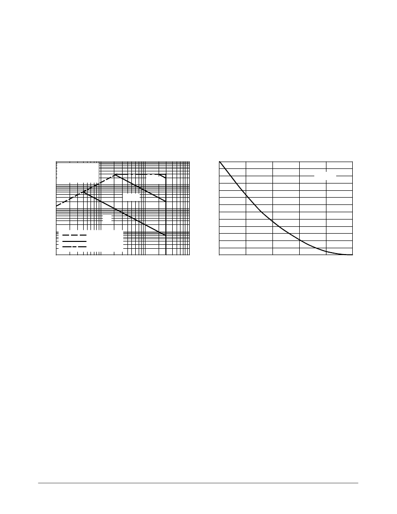
�SAFE� OPERATING� AREA�
�The� Forward� Biased� Safe� Operating� Area� curves� define�
�the� maximum� simultaneous� drain--to--source� voltage� and�
�drain� current� that� a� transistor� can� handle� safely� when� it� is�
�forward� biased.� Curves� are� based� upon� maximum� peak�
�junction� temperature� and� a� case� temperature� (T� C� )� of� 25� ?� C.�
�Peak� repetitive� pulsed� power� limits� are� determined� by� using�
�the� thermal� response� data� in� conjunction� with� the� procedures�
�discussed� in� AN569,� “Transient� Thermal� Resistance� --�
�General� Data� and� Its� Use.”�
�Switching� between� the� off--state� and� the� on--state� may�
�traverse� any� load� line� provided� neither� rated� peak� current�
�(I� DM� )� nor� rated� voltage� (V� DSS� )� is� exceeded,� and� that� the�
�transition� time� (t� r� ,� t� f� )� does� not� exceed� 10� m� s.� In� addition� the�
�total� power� averaged� over� a� complete� switching� cycle� must�
�not� exceed� (T� J(MAX)� --� T� C� )/(R� m� JC� ).�
�A� power� MOSFET� designated� E--FET� can� be� safely� used�
�in� switching� circuits� with� unclamped� inductive� loads.� For�
�reliable� operation,� the� stored� energy� from� circuit� inductance�
�dissipated� in� the� transistor� while� in� avalanche� must� be� less�
�than� the� rated� limit� and� must� be� adjusted� for� operating�
�conditions� differing� from� those� specified.� Although� industry�
�practice� is� to� rate� in� terms� of� energy,� avalanche� energy�
�capability� is� not� a� constant.� The� energy� rating� decreases�
�non--linearly� with� an� increase� of� peak� current� in� avalanche�
�and� peak� junction� temperature.�
�100�
�10�
�V� GS� =� 12� V�
�SINGLE� PULSE�
�T� A� =� 25� ?� C�
�1.0 ms�
�325�
�300�
�275�
�250�
�225�
�I� D� =� 6�
�A�
�1�
�dc�
�10� ms�
�200�
�175�
�150�
�125�
�0.1�
�R� DS(on)� LIMIT�
�THERMAL� LIMIT�
�100�
�75�
�50�
�0.01�
�0.1�
�PACKAGE� LIMIT�
�1.0�
�10�
�100�
�25�
�0�
�25�
�50�
�75�
�100�
�125�
�150�
�V� DS� ,� DRAIN--TO--SOURCE� VOLTAGE� (VOLTS)�
�Figure� 11.� Maximum� Rated� Forward� Biased�
�Safe� Operating� Area�
�T� J� ,� STARTING� JUNCTION� TEMPERATURE� (� ?� C)�
�Figure� 12.� Maximum� Avalanche� Energy� versus�
�Starting� Junction� Temperature�
�http://onsemi.com�
�6�
�相关PDF资料 |
PDF描述 |
|---|---|
| NTMD6P02R2G | MOSFET PWR P-CHAN DUAL 20V 8SOIC |
| NTMFD4901NFT1G | MOSFET N-CH DUAL 30V 8DFN |
| NTMFS4108NT1G | MOSFET N-CHAN 22A 30V SO-8FL |
| NTMFS4119NT1G | MOSFET N-CHAN 18A 30V SO-8FL |
| NTMFS4120NT1G | MOSFET N-CHAN 18A 30V SO-8FL |
相关代理商/技术参数 |
参数描述 |
|---|---|
| NTMD6N03R2G | 功能描述:MOSFET NFET 30V SPCL TR RoHS:否 制造商:STMicroelectronics 晶体管极性:N-Channel 汲极/源极击穿电压:650 V 闸/源击穿电压:25 V 漏极连续电流:130 A 电阻汲极/源极 RDS(导通):0.014 Ohms 配置:Single 最大工作温度: 安装风格:Through Hole 封装 / 箱体:Max247 封装:Tube |
| NTMD6N04R2 | 制造商:ONSEMI 制造商全称:ON Semiconductor 功能描述:Power MOSFET 40 V, 5.8 A, Dual N-Channel SOIC-8 |
| NTMD6N04R2G | 功能描述:MOSFET NFET SO8 40V 5.8A 0.027R RoHS:否 制造商:STMicroelectronics 晶体管极性:N-Channel 汲极/源极击穿电压:650 V 闸/源击穿电压:25 V 漏极连续电流:130 A 电阻汲极/源极 RDS(导通):0.014 Ohms 配置:Single 最大工作温度: 安装风格:Through Hole 封装 / 箱体:Max247 封装:Tube |
| NTMD6P02 | 制造商:ONSEMI 制造商全称:ON Semiconductor 功能描述:Power MOSFET 6 A, 20 V, Pa??Channel SOICa??8, Dual |
| NTMD6P02R2 | 功能描述:MOSFET 20V 6A P-Channel RoHS:否 制造商:STMicroelectronics 晶体管极性:N-Channel 汲极/源极击穿电压:650 V 闸/源击穿电压:25 V 漏极连续电流:130 A 电阻汲极/源极 RDS(导通):0.014 Ohms 配置:Single 最大工作温度: 安装风格:Through Hole 封装 / 箱体:Max247 封装:Tube |
发布紧急采购,3分钟左右您将得到回复。