- 您现在的位置:买卖IC网 > PDF目录224618 > NX25P16-VSI (WINBOND ELECTRONICS CORP) 16M X 1 FLASH 2.7V PROM, PDSO8 PDF资料下载
参数资料
| 型号: | NX25P16-VSI |
| 厂商: | WINBOND ELECTRONICS CORP |
| 元件分类: | PROM |
| 英文描述: | 16M X 1 FLASH 2.7V PROM, PDSO8 |
| 封装: | 0.208 INCH, SOIC-8 |
| 文件页数: | 9/43页 |
| 文件大小: | 918K |
| 代理商: | NX25P16-VSI |
第1页第2页第3页第4页第5页第6页第7页第8页当前第9页第10页第11页第12页第13页第14页第15页第16页第17页第18页第19页第20页第21页第22页第23页第24页第25页第26页第27页第28页第29页第30页第31页第32页第33页第34页第35页第36页第37页第38页第39页第40页第41页第42页第43页

W25P80 / W25P16 / W25P32
Publication Release Date: December 11, 2005
- 17 -
Revision J
9.2.5
Write Status Register (01h)
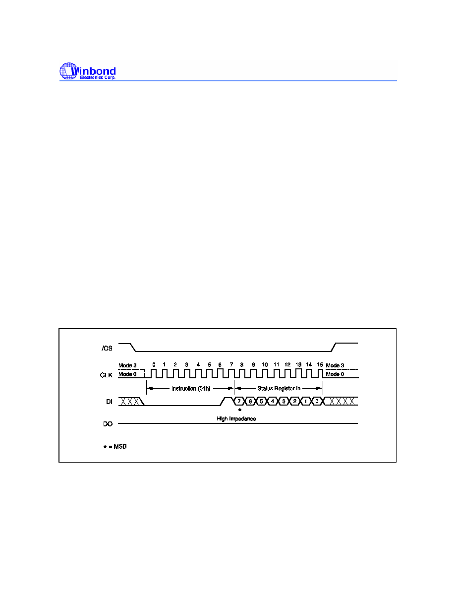
The Write Status Register instruction allows the Status Register to be written. A Write Enable
instruction must previously have been executed for the device to accept the Write Status Register
Instruction (Status Register bit WEL must equal 1). Once write enabled, the instruction is entered by
driving /CS low, sending the instruction code “01h”, and then writing the status register data byte as
illustrated in figure 7. The Status Register bits are shown in figure 3 and described earlier in this data
sheet.
Only non-volatile Status Register bits SRP, BP2, BP1 and BP0 (bits 7, 4, 3 and 2) can be written to.
All other Status Register bit locations are read-only and will not be affected by the Write Status
Register instruction.
The /CS pin must be driven high after the eighth bit of the last byte has been latched. If this is not
done the Write Status Register instruction will not be executed. After /CS is driven high, the self-timed
Write Status Register cycle will commence for a time duration of tW (See AC Characteristics). While
the Write Status Register cycle is in progress, the Read Status Register instruction may still accessed
to check the status of the BUSY bit. The BUSY bit is a 1 during the Write Status Register cycle and a
0 when the cycle is finished and ready to accept other instructions again. After the Write Register
cycle has finished the Write Enable Latch (WEL) bit in the Status Register will be cleared to 0.
The Write Status Register instruction allows the Block Protect bits (BP2, BP1 and BP0) to be set for
protecting all, a portion, or none of the memory from erase and program instructions. Protected areas
become read-only (see Status Register Memory Protection table). The Write Status Register
instruction also allows the Status Register Protect bit (SRP) to be set. This bit is used in conjunction
with the Write Protect (/WP) pin to disable writes to the status register. When the SRP bit is set to a 0
state (factory default) the /WP pin has no control over the status register. When the SRP pin is set to a
1, the Write Status Register instruction is locked out while the /WP pin is low. When the /WP pin is
high the Write Status Register instruction is allowed.
Figure 7. Write Status Register Instruction Sequence Diagram
相关PDF资料 |
PDF描述 |
|---|---|
| NX3225SA-100.000M-STD-CSR-3 | QUARTZ CRYSTAL RESONATOR, 100 MHz |
| NX5A0AE01 | MALE, STRAIGHT TWO PART BOARD CONNECTOR, PRESS FIT |
| NX5B0AE01 | MALE, STRAIGHT TWO PART BOARD CONNECTOR, PRESS FIT |
| NX5C0AE01 | MALE, STRAIGHT TWO PART BOARD CONNECTOR, PRESS FIT |
| NX5G0AE01 | MALE, STRAIGHT TWO PART BOARD CONNECTOR, PRESS FIT |
相关代理商/技术参数 |
参数描述 |
|---|---|
| NX25P20 | 制造商:未知厂家 制造商全称:未知厂家 功能描述:1M BIT 2M BIT AND 4M BIT SERIAL FLASH MEMORY WITH 10MHZ SPI |
| NX25P40 | 制造商:未知厂家 制造商全称:未知厂家 功能描述:1M BIT 2M BIT AND 4M BIT SERIAL FLASH MEMORY WITH 10MHZ SPI |
| NX-25TA-CV1 | 制造商:HRS 制造商全称:HRS 功能描述:I/O Card Interface Connectors |
| NX-25TA-CV1(50) | 功能描述:记忆卡连接器 PC CARD FRAME KIT ACCESRY PLUG CVR RoHS:否 制造商:Yamaichi Electronics 产品:Card Connectors 卡类型:microSD 类型: 节距: 方向: 安装风格:SMD/SMT 端接类型: 排数: 触点数量: 电流额定值:0.5 A 电压额定值:50 V |
| NX-25T-BS | 制造商:Hirose 功能描述:234-0074-0-00 EACH |
发布紧急采购,3分钟左右您将得到回复。