- 您现在的位置:买卖IC网 > PDF目录189449 > OR3L225B7PS680-DB (LATTICE SEMICONDUCTOR CORP) FPGA, 1444 CLBS, 166000 GATES, 266.4 MHz, PBGA680 PDF资料下载
参数资料
| 型号: | OR3L225B7PS680-DB |
| 厂商: | LATTICE SEMICONDUCTOR CORP |
| 元件分类: | FPGA |
| 英文描述: | FPGA, 1444 CLBS, 166000 GATES, 266.4 MHz, PBGA680 |
| 封装: | PLASTIC, BGAM-680 |
| 文件页数: | 4/77页 |
| 文件大小: | 873K |
| 代理商: | OR3L225B7PS680-DB |
第1页第2页第3页当前第4页第5页第6页第7页第8页第9页第10页第11页第12页第13页第14页第15页第16页第17页第18页第19页第20页第21页第22页第23页第24页第25页第26页第27页第28页第29页第30页第31页第32页第33页第34页第35页第36页第37页第38页第39页第40页第41页第42页第43页第44页第45页第46页第47页第48页第49页第50页第51页第52页第53页第54页第55页第56页第57页第58页第59页第60页第61页第62页第63页第64页第65页第66页第67页第68页第69页第70页第71页第72页第73页第74页第75页第76页第77页
12
PD78052, 78053, 78054, 78055, 78056, 78058
Data Sheet U12327EJ5V0DS00
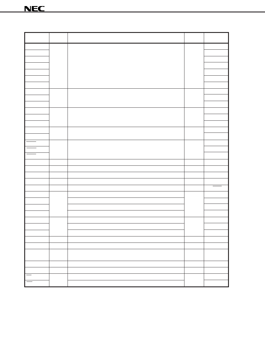
3.2 Non-Port Pins (1/2)
Pin Name
I/O
Function
After
Alternate
Reset
Function
INTP0
Input
External interrupt request input for which the valid edge (rising edge,
Input
P00/TI00
INTP1
falling edge, or both rising and falling edges) can be specified.
P01/TI01
INTP2
P02
INTP3
P03
INTP4
P04
INTP5
P05
INTP6
P06
SI0
Input
Serial interface serial data input
Input
P25/SB0
SI1
P20
SI2
P70/RxD
SO0
Output
Serial interface serial data output
Input
P26/SB1
SO1
P21
SO2
P71/TxD
SB0
I/O
Serial interface serial data input/output
Input
P25/SI0
SB1
P26/SO0
SCK0
I/O
Serial interface serial clock input/output
Input
P27
SCK1
P22
SCK2
P72/ASCK
STB
Output
Serial interface automatic transmit/receive strobe output
Input
P23
BUSY
Input
Serial interface automatic transmit/receive busy input
Input
P24
RxD
Input
Asynchronous serial interface serial data input
Input
P70/SI2
TxD
Output
Asynchronous serial interface serial data output
Input
P71/SO2
ASCK
Input
Asynchronous serial interface serial clock input
Input
P72/SCK2
TI00
Input
External count clock input to the 16-bit timer (TM0)
Input
P00/INTP0
TI01
Capture trigger signal input to the capture register (CR00)
P01/INTP1
TI1
External count clock input to the 8-bit timer (TM1)
P33
TI2
External count clock input to the 8-bit timer (TM2)
P34
TO0
Output
16-bit timer (TM0) output (also used for 14-bit PWM output)
Input
P30
TO1
8-bit timer (TM1) output
P31
TO2
8-bit timer (TM2) output
P32
PCL
Output
Clock output (for trimming of main system clock and subsystem clock)
Input
P35
BUZ
Output
Buzzer output
Input
P36
RTP0 to RTP7 Output
Real-time output port from which data is output in synchronization with
Input
P120 to P127
a trigger
AD0 to AD7
I/O
Lower address/data bus for expanding memory externally
Input
P40 to P47
A8 to A15
Output
Higher address bus for expanding memory externally
Input
P50 to P57
RD
Output
Strobe signal output for reading from external memory
Input
P64
WR
Strobe signal output for writing to external memory
P65
相关PDF资料 |
PDF描述 |
|---|---|
| OR3L225B7PS680I-DB | FPGA, 1444 CLBS, 166000 GATES, 266.4 MHz, PBGA680 |
| OR3L225B8PS432-DB | FPGA, 1444 CLBS, 166000 GATES, 333 MHz, PBGA432 |
| OR3L225B8PS680-DB | FPGA, 1444 CLBS, 166000 GATES, 333 MHz, PBGA680 |
| OR3L225B7BC432-DB | FPGA, 1444 CLBS, 166000 GATES, 266.4 MHz, PBGA432 |
| OR3L225B8BC432-DB | FPGA, 1444 CLBS, 166000 GATES, 333 MHz, PBGA432 |
相关代理商/技术参数 |
参数描述 |
|---|---|
| OR3L225B8BC432-DB | 功能描述:FPGA - 现场可编程门阵列 11552 LUT 612 I/O RoHS:否 制造商:Altera Corporation 系列:Cyclone V E 栅极数量: 逻辑块数量:943 内嵌式块RAM - EBR:1956 kbit 输入/输出端数量:128 最大工作频率:800 MHz 工作电源电压:1.1 V 最大工作温度:+ 70 C 安装风格:SMD/SMT 封装 / 箱体:FBGA-256 |
| OR3L225B8BM680-DB | 功能描述:FPGA - 现场可编程门阵列 11552 LUT 612 I/O RoHS:否 制造商:Altera Corporation 系列:Cyclone V E 栅极数量: 逻辑块数量:943 内嵌式块RAM - EBR:1956 kbit 输入/输出端数量:128 最大工作频率:800 MHz 工作电源电压:1.1 V 最大工作温度:+ 70 C 安装风格:SMD/SMT 封装 / 箱体:FBGA-256 |
| OR3LP26B | 制造商:AGERE 制造商全称:AGERE 功能描述:Field-Programmable System Chip (FPSC) Embedded Master/Target PCI Interface |
| OR3LP26BBA352-DB | 功能描述:FPGA - 现场可编程门阵列 FPSC PCI INTERFACE RoHS:否 制造商:Altera Corporation 系列:Cyclone V E 栅极数量: 逻辑块数量:943 内嵌式块RAM - EBR:1956 kbit 输入/输出端数量:128 最大工作频率:800 MHz 工作电源电压:1.1 V 最大工作温度:+ 70 C 安装风格:SMD/SMT 封装 / 箱体:FBGA-256 |
| OR3LP26BBM680-DB | 功能描述:FPGA - 现场可编程门阵列 FPSC PCI INTERFACE RoHS:否 制造商:Altera Corporation 系列:Cyclone V E 栅极数量: 逻辑块数量:943 内嵌式块RAM - EBR:1956 kbit 输入/输出端数量:128 最大工作频率:800 MHz 工作电源电压:1.1 V 最大工作温度:+ 70 C 安装风格:SMD/SMT 封装 / 箱体:FBGA-256 |
发布紧急采购,3分钟左右您将得到回复。