- 您现在的位置:买卖IC网 > PDF目录189449 > OR3L225B7PS680-DB (LATTICE SEMICONDUCTOR CORP) FPGA, 1444 CLBS, 166000 GATES, 266.4 MHz, PBGA680 PDF资料下载
参数资料
| 型号: | OR3L225B7PS680-DB |
| 厂商: | LATTICE SEMICONDUCTOR CORP |
| 元件分类: | FPGA |
| 英文描述: | FPGA, 1444 CLBS, 166000 GATES, 266.4 MHz, PBGA680 |
| 封装: | PLASTIC, BGAM-680 |
| 文件页数: | 45/77页 |
| 文件大小: | 873K |
| 代理商: | OR3L225B7PS680-DB |
第1页第2页第3页第4页第5页第6页第7页第8页第9页第10页第11页第12页第13页第14页第15页第16页第17页第18页第19页第20页第21页第22页第23页第24页第25页第26页第27页第28页第29页第30页第31页第32页第33页第34页第35页第36页第37页第38页第39页第40页第41页第42页第43页第44页当前第45页第46页第47页第48页第49页第50页第51页第52页第53页第54页第55页第56页第57页第58页第59页第60页第61页第62页第63页第64页第65页第66页第67页第68页第69页第70页第71页第72页第73页第74页第75页第76页第77页
4
Lattice Semiconductor
Data Addendum
March 2002
ORCA OR3LxxxB Series FPGAs
Features (continued)
■ Programmable I/O (PIO) has:
— Fast-capture input latch and input ip-op (FF)/
latch for reduced input setup time and zero hold
time.
— Capability to (de)multiplex I/O signals.
— Fast access to SLIC for decodes and
PAL-like
functions.
— Output FF and two-signal function generator to
reduce CLK to output propagation delay.
— Fast open-drain drive capability.
■ New programmable I/O 3-state FF allows 3-state
buffer control signals to be set up a clock cycle early
for improved clock to output delays.
System-Level Features
System-level features reduce glue logic requirements
and make a system on a chip possible. These features
in the
ORCA OR3LxxxB include the following:
■ Full PCI local bus compliance for all devices in
3.3 V and 5 V PCI systems. Pin-selectable I/O
clamping diodes provide 3.3 V and 5 V compliance
and 5 V tolerance.
■ Dual-use microprocessor interface (MPI) can be
used for conguration, readback, device control, and
device status, as well as for a general-purpose inter-
face to the FPGA. Glueless interface to
i960 * and
PowerPC processors with user-congurable
address space provided.
■ Parallel readback of conguration data capability with
the built-in microprocessor interface.
■ Programmable clock manager (PCM) adjusts clock
phase and duty cycle for input clock rates from
5 MHz to 120 MHz. The PCM may be combined with
FPGA logic to create complex functions, such as dig-
ital phase-locked loops (DPLL), frequency counters,
and frequency synthesizers. Two PCMs are provided
per device.
■ True internal 3-state, bidirectional buses with simple
control provided by the SLIC.
■ 32
× 4 RAM per PFU, congurable as single- or dual-
port. Create large, fast RAM/ROM blocks (128
× 8 in
only eight PFUs) using the SLIC decoders as bank
drivers.
■ Full UTOPIA Level III I/O compliance (6.0 ns
CLK -> OUT, 2.0 ns setup with 0 ns hold).
*
i960 is a registered trademark of Intel Corporation.
PowerPC is a registered trademark of International Business
Machines, Inc.
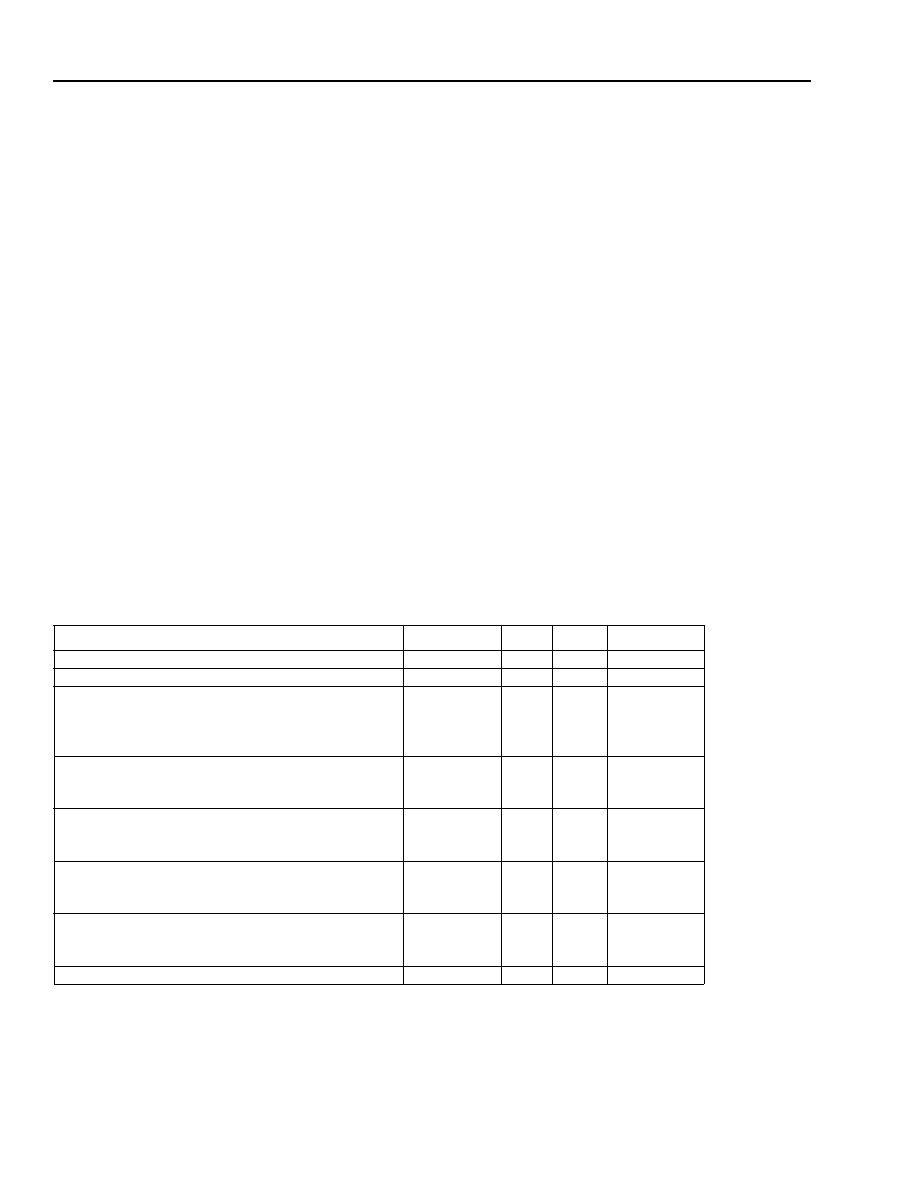
Table 2
. ORCA Series 3L System Performance
1. Implemented using 8
× 1 multiplier mode (unpipelined), register-to-register, two 8-bit inputs, one 16-bit output.
2. Implemented using two 32
× 12 ROMs and one 12-bit adder, one 8-bit input, one xed operand, one 16-bit output.
3. Implemented using 8
× 1 multiplier mode (fully pipelined), two 8-bit inputs, one 16-bit output (seven of 15 PFUs contain
only pipelining registers).
4. Implemented using 32
× 4 RAM mode with read data on 3-state buffer to bidirectional read/write bus.
5. Implemented using 32
× 4 dual-port RAM mode.
6. Implemented in one partially occupied SLIC with decoded output set up to CE in same PLC.
7. Implemented in ve partially occupied SLICs.
Parameter
# PFUs
-7
-8
Unit
16-bit Loadable Up/Down Counter
2
151
176
MHz
16-bit Accumulator
2
151
176
MHz
8
× 8 Parallel Multiplier:
Multiplier Mode, Unpipelined1
ROM Mode, Unpipelined2
Multiplier Mode, Pipelined3
11.5
8
15
38
93
129
46
116
152
MHz
32
× 16 RAM (synchronous):
Single-port, 3-state Bus4
Dual-port5
4
173
231
209
277
MHz
128
× 8 RAM (synchronous):
Single-port, 3-state Bus4
Dual-port5
8
151
181
MHz
8-bit Address Decode (internal):
Using Softwired LUTs
Using SLICs6
0.25
0
2.30
1.29
2.00
1.12
ns
32-bit Address Decode (internal):
Using Softwired LUTs
Using SLICs7
2
0
7.97
3.75
6.84
3.16
ns
36-bit Parity Check (internal)
2
7.97
6.84
ns
ALL
DEVICES
DISCONTINUED
相关PDF资料 |
PDF描述 |
|---|---|
| OR3L225B7PS680I-DB | FPGA, 1444 CLBS, 166000 GATES, 266.4 MHz, PBGA680 |
| OR3L225B8PS432-DB | FPGA, 1444 CLBS, 166000 GATES, 333 MHz, PBGA432 |
| OR3L225B8PS680-DB | FPGA, 1444 CLBS, 166000 GATES, 333 MHz, PBGA680 |
| OR3L225B7BC432-DB | FPGA, 1444 CLBS, 166000 GATES, 266.4 MHz, PBGA432 |
| OR3L225B8BC432-DB | FPGA, 1444 CLBS, 166000 GATES, 333 MHz, PBGA432 |
相关代理商/技术参数 |
参数描述 |
|---|---|
| OR3L225B8BC432-DB | 功能描述:FPGA - 现场可编程门阵列 11552 LUT 612 I/O RoHS:否 制造商:Altera Corporation 系列:Cyclone V E 栅极数量: 逻辑块数量:943 内嵌式块RAM - EBR:1956 kbit 输入/输出端数量:128 最大工作频率:800 MHz 工作电源电压:1.1 V 最大工作温度:+ 70 C 安装风格:SMD/SMT 封装 / 箱体:FBGA-256 |
| OR3L225B8BM680-DB | 功能描述:FPGA - 现场可编程门阵列 11552 LUT 612 I/O RoHS:否 制造商:Altera Corporation 系列:Cyclone V E 栅极数量: 逻辑块数量:943 内嵌式块RAM - EBR:1956 kbit 输入/输出端数量:128 最大工作频率:800 MHz 工作电源电压:1.1 V 最大工作温度:+ 70 C 安装风格:SMD/SMT 封装 / 箱体:FBGA-256 |
| OR3LP26B | 制造商:AGERE 制造商全称:AGERE 功能描述:Field-Programmable System Chip (FPSC) Embedded Master/Target PCI Interface |
| OR3LP26BBA352-DB | 功能描述:FPGA - 现场可编程门阵列 FPSC PCI INTERFACE RoHS:否 制造商:Altera Corporation 系列:Cyclone V E 栅极数量: 逻辑块数量:943 内嵌式块RAM - EBR:1956 kbit 输入/输出端数量:128 最大工作频率:800 MHz 工作电源电压:1.1 V 最大工作温度:+ 70 C 安装风格:SMD/SMT 封装 / 箱体:FBGA-256 |
| OR3LP26BBM680-DB | 功能描述:FPGA - 现场可编程门阵列 FPSC PCI INTERFACE RoHS:否 制造商:Altera Corporation 系列:Cyclone V E 栅极数量: 逻辑块数量:943 内嵌式块RAM - EBR:1956 kbit 输入/输出端数量:128 最大工作频率:800 MHz 工作电源电压:1.1 V 最大工作温度:+ 70 C 安装风格:SMD/SMT 封装 / 箱体:FBGA-256 |
发布紧急采购,3分钟左右您将得到回复。