- 您现在的位置:买卖IC网 > PDF目录189449 > OR3T55 3C and 3T Field-Programmable Gate Arrays PDF资料下载
参数资料
| 型号: | OR3T55 |
| 英文描述: | 3C and 3T Field-Programmable Gate Arrays |
| 中文描述: | 3C和3吨现场可编程门阵列 |
| 文件页数: | 163/210页 |
| 文件大小: | 4669K |
| 代理商: | OR3T55 |
第1页第2页第3页第4页第5页第6页第7页第8页第9页第10页第11页第12页第13页第14页第15页第16页第17页第18页第19页第20页第21页第22页第23页第24页第25页第26页第27页第28页第29页第30页第31页第32页第33页第34页第35页第36页第37页第38页第39页第40页第41页第42页第43页第44页第45页第46页第47页第48页第49页第50页第51页第52页第53页第54页第55页第56页第57页第58页第59页第60页第61页第62页第63页第64页第65页第66页第67页第68页第69页第70页第71页第72页第73页第74页第75页第76页第77页第78页第79页第80页第81页第82页第83页第84页第85页第86页第87页第88页第89页第90页第91页第92页第93页第94页第95页第96页第97页第98页第99页第100页第101页第102页第103页第104页第105页第106页第107页第108页第109页第110页第111页第112页第113页第114页第115页第116页第117页第118页第119页第120页第121页第122页第123页第124页第125页第126页第127页第128页第129页第130页第131页第132页第133页第134页第135页第136页第137页第138页第139页第140页第141页第142页第143页第144页第145页第146页第147页第148页第149页第150页第151页第152页第153页第154页第155页第156页第157页第158页第159页第160页第161页第162页当前第163页第164页第165页第166页第167页第168页第169页第170页第171页第172页第173页第174页第175页第176页第177页第178页第179页第180页第181页第182页第183页第184页第185页第186页第187页第188页第189页第190页第191页第192页第193页第194页第195页第196页第197页第198页第199页第200页第201页第202页第203页第204页第205页第206页第207页第208页第209页第210页
56
Lucent Technologies Inc.
Data Sheet
June 1999
ORCA Series 3C and 3T FPGAs
Special Function Blocks (continued)
Start-Up Logic
The start-up logic block is located in the lower right cor-
ner of the FPGA. This block can be configured to coor-
dinate the relative timing of the release of GSRN, the
activation of all user I/Os, and the assertion of the
DONE signal at the end of configuration. If a start-up
clock is used to time these events, the start-up clock
can come from CCLK, or it can be routed into the start-
up block using lower right corner routing resources.
These signals are described in the Start-Up subsection
of the FPGA States of Operation section.
Clock Control (CLKCNTRL) and StopCLK
There is one CLKCNTRL block in the MID section of
the interquad routing on each side of the FPGA. This
block is used to selectively distribute the fast clock to
the PLC array and the left (top) and right (bottom)
ExpressCLKs (ECKL and ECKR) to the side of the
array on which the CLKCNTRL block resides.
The source clock for the CLKCNTRL block comes
either from the ExpressCLK pad at the middle of the
side of the FPGA or from the corner ExpressCLK route
that comes from the corner ExpressCLK pad (at the
lower left or upper right of the device, whichever is
closer). The programmable clock manager ExpressCLK
output can also be sourced to this corner routing for
distribution at the two closest CLKCNTRL blocks.
Each CLKCNTRL block also features an invertible
StopCLK
shutoff input that is available from local rout-
ing. This feature may be used to glitchlessly stop and
start the clock at the three outputs of each CLKCNTRL
block and has the option of doing so on either the rising
or falling edge of the clock. When the clock is halted
based on its rising edge, it stops and stays at VDD.
When it is stopped based on its falling edge, it stops
and stays at GND. If the StopCLK shutoff signal meets
the CLKCNTRL setup and hold times, the clock is
stopped on the second clock cycle after the shutoff sig-
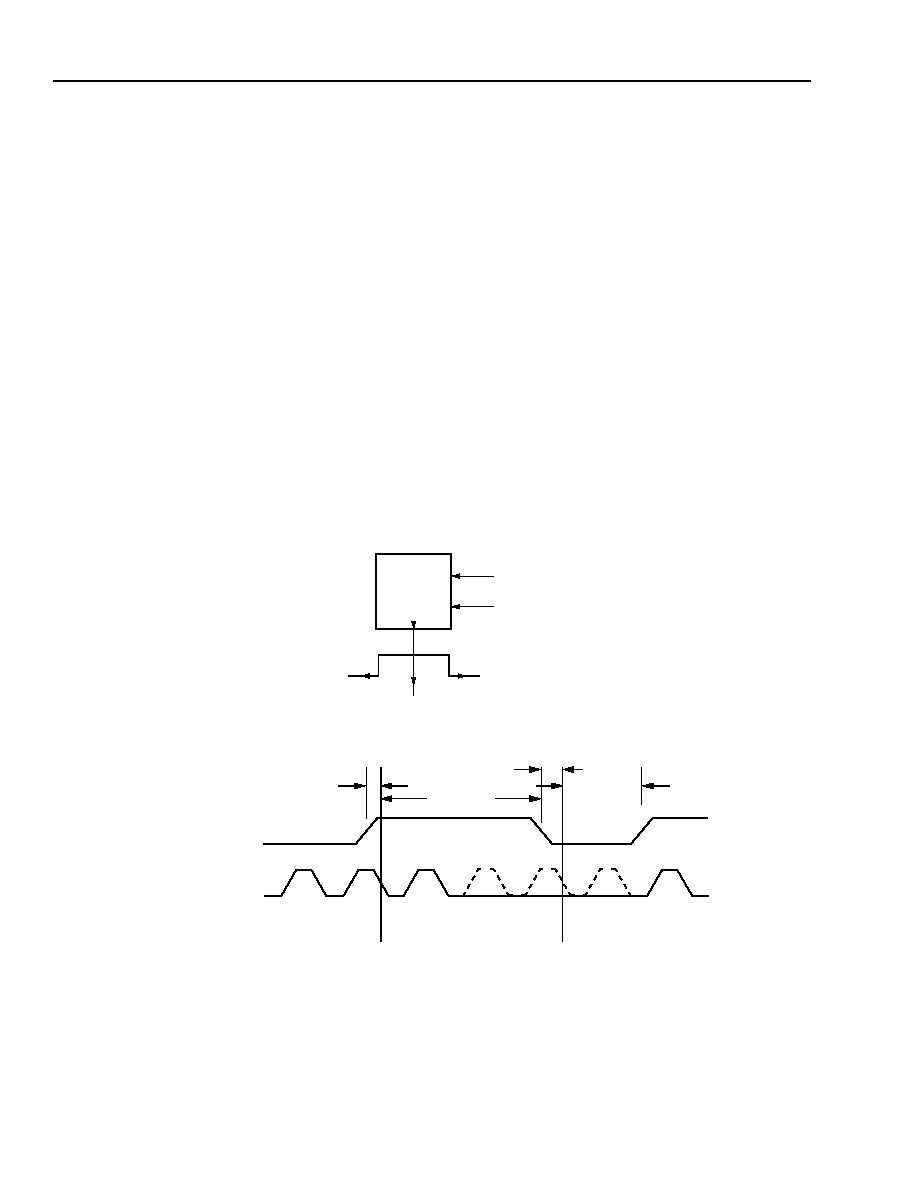
nal. A diagram of the bottom CLKCNTRL block and
StopCLK
timing is shown in Figure 35.
5-5981(F)
Notes:
CLKCNTRL output clocks are ExpressCLK left and right and fast clock.
Clock shutoff shown active-high acting on clock falling edge.
Figure 35. Top CLKCNTRL Function Block
CORNER EXPRESSCLK
CLOCK SHUTOFF
EXPRESSCLK RIGHT
EXPRESSCLK LEFT
FAST CLOCK
CLOCK SHUTOFF
OFF_SET
OFF_HLD
OFF_SET
OFF_HLD
CLKCNTRL OUTPUT
CLOCKS
相关PDF资料 |
PDF描述 |
|---|---|
| OR4E041BA352-DB | FPGA, 1296 CLBS, 380000 GATES, PBGA352 |
| OR4E041BM416-DB | FPGA, 1296 CLBS, 380000 GATES, PBGA416 |
| OR4E041BM680-DB | FPGA, 1296 CLBS, 380000 GATES, PBGA680 |
| OR4E042BA352-DB | FPGA, 1296 CLBS, 380000 GATES, PBGA352 |
| OR4E042BM416-DB | FPGA, 1296 CLBS, 380000 GATES, PBGA416 |
相关代理商/技术参数 |
参数描述 |
|---|---|
| OR3T55-4BA256I | 制造商:未知厂家 制造商全称:未知厂家 功能描述:Field Programmable Gate Array (FPGA) |
| OR3T55-4PS208I | 制造商:未知厂家 制造商全称:未知厂家 功能描述:Field Programmable Gate Array (FPGA) |
| OR3T55-4PS240I | 制造商:未知厂家 制造商全称:未知厂家 功能描述:Field Programmable Gate Array (FPGA) |
| OR3T55-5BA256 | 制造商:AGERE 制造商全称:AGERE 功能描述:3C and 3T Field-Programmable Gate Arrays |
| OR3T55-5BA256I | 制造商:AGERE 制造商全称:AGERE 功能描述:3C and 3T Field-Programmable Gate Arrays |
发布紧急采购,3分钟左右您将得到回复。