- 您现在的位置:买卖IC网 > PDF目录189449 > OR4E041BA352-DB (LATTICE SEMICONDUCTOR CORP) FPGA, 1296 CLBS, 380000 GATES, PBGA352 PDF资料下载
参数资料
| 型号: | OR4E041BA352-DB |
| 厂商: | LATTICE SEMICONDUCTOR CORP |
| 元件分类: | FPGA |
| 英文描述: | FPGA, 1296 CLBS, 380000 GATES, PBGA352 |
| 封装: | PLASTIC, BGA-352 |
| 文件页数: | 143/151页 |
| 文件大小: | 2680K |
| 代理商: | OR4E041BA352-DB |
第1页第2页第3页第4页第5页第6页第7页第8页第9页第10页第11页第12页第13页第14页第15页第16页第17页第18页第19页第20页第21页第22页第23页第24页第25页第26页第27页第28页第29页第30页第31页第32页第33页第34页第35页第36页第37页第38页第39页第40页第41页第42页第43页第44页第45页第46页第47页第48页第49页第50页第51页第52页第53页第54页第55页第56页第57页第58页第59页第60页第61页第62页第63页第64页第65页第66页第67页第68页第69页第70页第71页第72页第73页第74页第75页第76页第77页第78页第79页第80页第81页第82页第83页第84页第85页第86页第87页第88页第89页第90页第91页第92页第93页第94页第95页第96页第97页第98页第99页第100页第101页第102页第103页第104页第105页第106页第107页第108页第109页第110页第111页第112页第113页第114页第115页第116页第117页第118页第119页第120页第121页第122页第123页第124页第125页第126页第127页第128页第129页第130页第131页第132页第133页第134页第135页第136页第137页第138页第139页第140页第141页第142页当前第143页第144页第145页第146页第147页第148页第149页第150页第151页
Lattice Semiconductor
91
Data Sheet
September, 2002
ORCA Series 4 FPGAs
TimingCharacteristics(continued)
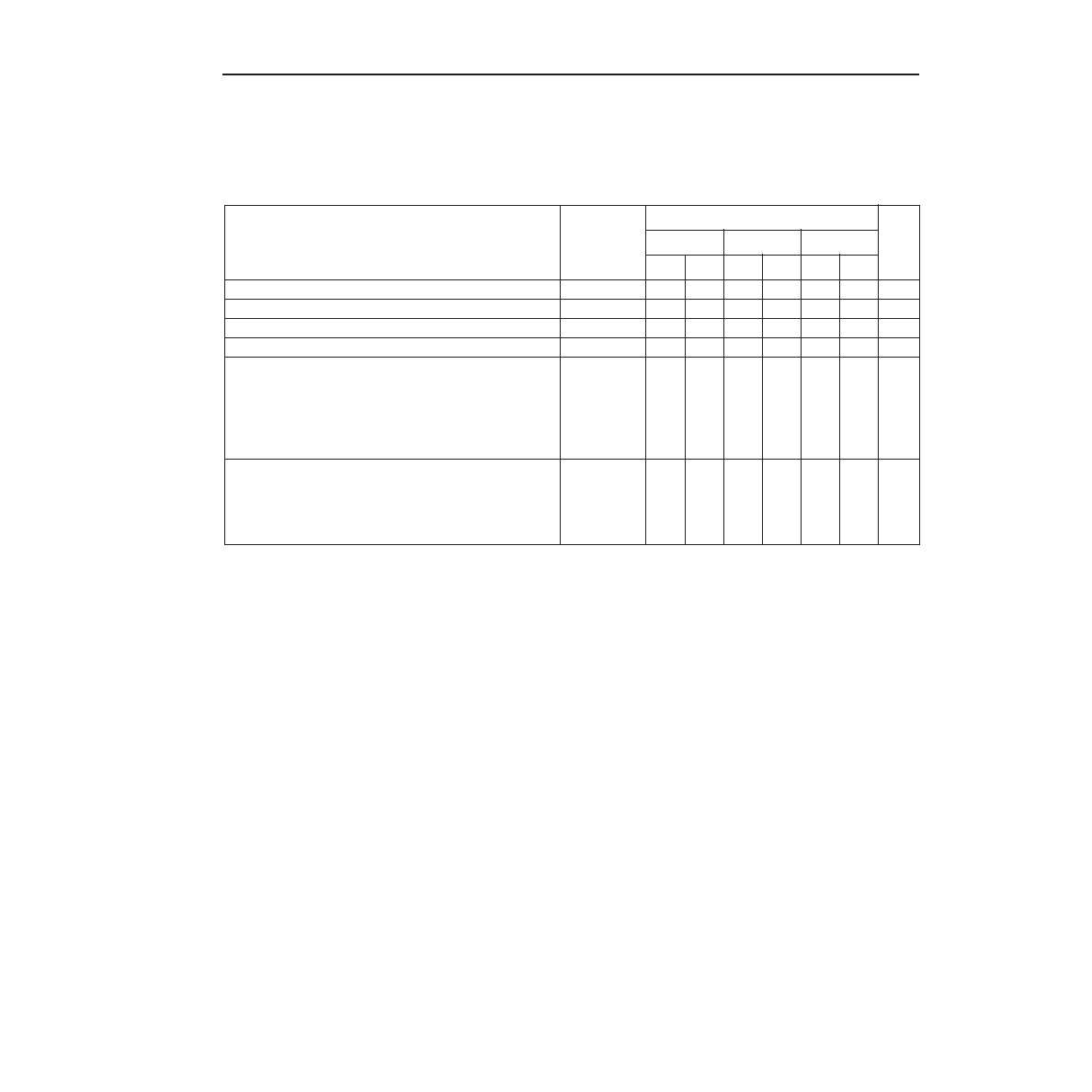
Table56.PrimaryCLK(PCLK)Setup/HoldTimeusingon-chipPLLs(Pin-to-Pin)
OR4Exxx industrial: VDD15 = 1.425 V to 1.575 V, VDD33 = 3.0 V to 3.6 V, VDDIO = 3.0 V to 3.6 V, –40 °C
< TJ
< +85 °C.
Notes:
1. Thepin-to-pintimingparametersinthistablewillmatchORCAFoundryiftheclockdelaymultiplierinthesetuppreferenceissetto0.95for
setuptimeand1.05forholdtime.
2. TimingusestheautomaticdelaycompensationmodeofthePLLs.ThefeedbacktothePLLisprovidedbytheglobalsystemclockrouting.
OtherdelayvaluesarepossiblebyusingthephasemodificationsmodeofthePLLinstead.
3. Thissetup/holdtimeisforafullyroutedclocktreethatusestheprimaryclocknetwork.ItincludesboththeLVTTL(3.3V)inputclockbuffer
delay,PLLblock,theclockroutingtothePIOCLKinput,thesetup/holdtimeofthePIOFF(withthedatainputdelaydisabled)andthe
LVTTL(3.3V)inputdatabuffertoPIOFFdelay.ThePCLKinputclockisconnectedatthesemi-dedicatedPLLinputpin.
4. NotethatthePIOcyclestealingdelayadjustmentsandthePLLcyclestealingdelayadjustmentsareeachattemptingtopullthesameclock
inbothdirections.Ifbotharebeingused,thenthedifferencebetweenthemwillprovidethebasisforPIOsetupandholdtimes.
5. FortimingimprovementsusingotherI/Obuffertypesfortheinputclockbufferorinputdatabuffer,seeTable45.
Description
Device
Speed
Unit
-1
-2
-3
Min Max Min Max Min Max
Input to PCLK Setup Time, Input Data Delay Enabled
All
7.73
—
7.30
—
6.66
—
ns
Input to PCLK Setup Time, No Input Data Delay
All
0.00
—
0.00
—
0.00
—
ns
Input to PCLK Hold Time, Input Data Delay Enabled
All
0.00
—
0.00
—
0.00
—
ns
Input to PCLK Hold Time, No Input Data Delay
All
1.82
—
1.73
—
1.57
—
ns
Input Delay Adjustments from PIO Cycle Stealing
(typically used to reduce setup time by the min value
shown):
One Delay Cell
Two Delay Cells
Three Delay Cells
ICYCDEL1
ICYCDEL2
ICYCDEL3
—
0.89
1.64
2.43
—
0.70
1.29
1.98
—
0.64
1.18
1.80
ns
PLL Delay Adjustments from Cycle Stealing (used to
reduce hold by the min delay value shown):
One Delay Cell
Two Delay Cells
Three Delay Cells
PLLCDEL1
PLLCDEL2
PLLCDEL3
—
0.89
1.64
2.43
—
0.70
1.29
1.98
—
0.64
1.18
1.80
ns
相关PDF资料 |
PDF描述 |
|---|---|
| OR4E041BM416-DB | FPGA, 1296 CLBS, 380000 GATES, PBGA416 |
| OR4E041BM680-DB | FPGA, 1296 CLBS, 380000 GATES, PBGA680 |
| OR4E042BA352-DB | FPGA, 1296 CLBS, 380000 GATES, PBGA352 |
| OR4E042BM416-DB | FPGA, 1296 CLBS, 380000 GATES, PBGA416 |
| OR4E042BM680-DB | FPGA, 1296 CLBS, 380000 GATES, PBGA680 |
相关代理商/技术参数 |
参数描述 |
|---|---|
| OR4E04-1BA352I | 功能描述:FPGA - 现场可编程门阵列 10368 LUT 466 I/O RoHS:否 制造商:Altera Corporation 系列:Cyclone V E 栅极数量: 逻辑块数量:943 内嵌式块RAM - EBR:1956 kbit 输入/输出端数量:128 最大工作频率:800 MHz 工作电源电压:1.1 V 最大工作温度:+ 70 C 安装风格:SMD/SMT 封装 / 箱体:FBGA-256 |
| OR4E04-1BM416C | 功能描述:FPGA - 现场可编程门阵列 10368 LUT 466 I/O RoHS:否 制造商:Altera Corporation 系列:Cyclone V E 栅极数量: 逻辑块数量:943 内嵌式块RAM - EBR:1956 kbit 输入/输出端数量:128 最大工作频率:800 MHz 工作电源电压:1.1 V 最大工作温度:+ 70 C 安装风格:SMD/SMT 封装 / 箱体:FBGA-256 |
| OR4E04-1BM416I | 功能描述:FPGA - 现场可编程门阵列 10368 LUT 466 I/O RoHS:否 制造商:Altera Corporation 系列:Cyclone V E 栅极数量: 逻辑块数量:943 内嵌式块RAM - EBR:1956 kbit 输入/输出端数量:128 最大工作频率:800 MHz 工作电源电压:1.1 V 最大工作温度:+ 70 C 安装风格:SMD/SMT 封装 / 箱体:FBGA-256 |
| OR4E04-1BM680C | 功能描述:FPGA - 现场可编程门阵列 10368 LUT 466 I/O RoHS:否 制造商:Altera Corporation 系列:Cyclone V E 栅极数量: 逻辑块数量:943 内嵌式块RAM - EBR:1956 kbit 输入/输出端数量:128 最大工作频率:800 MHz 工作电源电压:1.1 V 最大工作温度:+ 70 C 安装风格:SMD/SMT 封装 / 箱体:FBGA-256 |
| OR4E04-1BM680I | 功能描述:FPGA - 现场可编程门阵列 10368 LUT 466 I/O RoHS:否 制造商:Altera Corporation 系列:Cyclone V E 栅极数量: 逻辑块数量:943 内嵌式块RAM - EBR:1956 kbit 输入/输出端数量:128 最大工作频率:800 MHz 工作电源电压:1.1 V 最大工作温度:+ 70 C 安装风格:SMD/SMT 封装 / 箱体:FBGA-256 |
发布紧急采购,3分钟左右您将得到回复。