- 您现在的位置:买卖IC网 > PDF目录189449 > OR4E041BM416-DB (LATTICE SEMICONDUCTOR CORP) FPGA, 1296 CLBS, 380000 GATES, PBGA416 PDF资料下载
参数资料
| 型号: | OR4E041BM416-DB |
| 厂商: | LATTICE SEMICONDUCTOR CORP |
| 元件分类: | FPGA |
| 英文描述: | FPGA, 1296 CLBS, 380000 GATES, PBGA416 |
| 封装: | PLASTIC, FBGA-416 |
| 文件页数: | 2/151页 |
| 文件大小: | 2680K |
| 代理商: | OR4E041BM416-DB |
第1页当前第2页第3页第4页第5页第6页第7页第8页第9页第10页第11页第12页第13页第14页第15页第16页第17页第18页第19页第20页第21页第22页第23页第24页第25页第26页第27页第28页第29页第30页第31页第32页第33页第34页第35页第36页第37页第38页第39页第40页第41页第42页第43页第44页第45页第46页第47页第48页第49页第50页第51页第52页第53页第54页第55页第56页第57页第58页第59页第60页第61页第62页第63页第64页第65页第66页第67页第68页第69页第70页第71页第72页第73页第74页第75页第76页第77页第78页第79页第80页第81页第82页第83页第84页第85页第86页第87页第88页第89页第90页第91页第92页第93页第94页第95页第96页第97页第98页第99页第100页第101页第102页第103页第104页第105页第106页第107页第108页第109页第110页第111页第112页第113页第114页第115页第116页第117页第118页第119页第120页第121页第122页第123页第124页第125页第126页第127页第128页第129页第130页第131页第132页第133页第134页第135页第136页第137页第138页第139页第140页第141页第142页第143页第144页第145页第146页第147页第148页第149页第150页第151页
10
Lattice Semiconductor
Data Sheet
September, 2002
ORCA Series 4 FPGAs
Programmable Logic Cells (continued)
Look-Up Table Operating Modes
The operating mode affects the functionality of the PFU input and output ports and internal PFU routing. For exam-
ple, in some operating modes, the DIN[7:0] inputs are direct data inputs to the PFU latches/FFs. In memory mode,
the same DIN[7:0] inputs are used as a 4-bit write data input bus and a 4-bit write address input bus into LUT
memory.
Table 2 lists the basic operating modes of the LUT. Figure 4—Figure 7 show block diagrams of the LUT operating
modes. The accompanying descriptions demonstrate each mode’s use for generating logic.
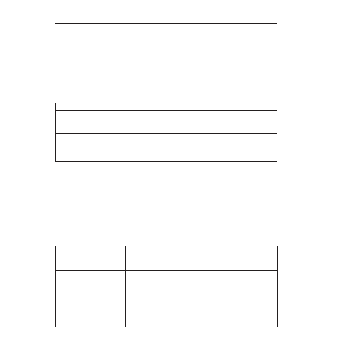
Table 2. Look-Up Table Operating Modes
PFU Control Inputs
Each PFU has eight routable control inputs and an active-low, asynchronous global set/reset (GSRN) signal that
affects all latches and FFs in the device. The eight control inputs are CLK[1:0], LSR[1:0], CE[1:0], and SEL[1:0],
and their functionality for each logic mode of the PFU is shown in Table 3. The clock signal to the PFU is CLK, CE
stands for clock enable, which is its primary function. LSR is the local set/reset signal that can be congured as
synchronous or asynchronous. The selection of set or reset is made for each latch/FF and is not a function of the
signal itself. SEL is used to dynamically select between direct PFU input and LUT output data as the input to
the latches/FFs.
All of the control signals can be disabled and/or inverted via the conguration logic. A disabled clock enable
indicates that the clock is always enabled. A disabled LSR indicates that the latch/FF never sets/resets (except
from GSRN). A disabled SEL input indicates that DIN[7:0] PFU inputs are routed to the latches/FFs.
Table 3. Control Input Functionality
Mode
Function
Logic
4-, 5-, and 6-input LUTs; softwired LUTs; latches/FFs with direct input or LUT input; CIN as direct
input to ninth FF or as pass through to COUT.
Half Logic/
Half Ripple
Upper four LUTs and latches/FFs in logic mode; lower four LUTs and latches/FFs in ripple mode;
CIN and ninth FF for logic or ripple functions.
Ripple
All LUTs combined to perform ripple-through data functions. Eight LUT registers available for
direct-in use or to register ripple output. Ninth FF dedicated to ripple out, if used. The submodes of
ripple mode are adder/subtractor, counter, multiplier, and comparator.
Memory
All LUTs and latches/FFs used to create a 32x4 synchronous dual-port RAM. Can be used as
single-port or as ROM.
Mode
CLK[1:0]
LSR[1:0]
CE[1:0]
SEL[1:0]
Logic
CLK to all latches/
FFs
LSR to all latches/FFs,
enabled per nibble and
for ninth FF
CE to all latches/FFs,
selectable per nibble
and for ninth FF
Select between LUT
input and direct input for
eight latches/FFs
Half Logic/
Half Ripple
CLK to all latches/
FFs
LSR to all latches/FF,
enabled per nibble and
for ninth FF
CE to all latches/FFs,
selectable per nibble
and for ninth FF
Select between LUT
input and direct input for
eight latches/FFs
Ripple
CLK to all latches/
FFs
LSR to all latches/FFs,
enabled per nibble and
for ninth FF
CE to all latches/FFs,
selectable per nibble
and for ninth FF
Select between LUT
input and direct input for
eight latches/FFs
Memory
(RAM)
CLK to RAM
LSR0 Port enable 2
CE1 RAM write enable
CE0 Port enable 1
Not used
Memory
(ROM)
Optional for
synchronous outputs
Not used
相关PDF资料 |
PDF描述 |
|---|---|
| OR4E041BM680-DB | FPGA, 1296 CLBS, 380000 GATES, PBGA680 |
| OR4E042BA352-DB | FPGA, 1296 CLBS, 380000 GATES, PBGA352 |
| OR4E042BM416-DB | FPGA, 1296 CLBS, 380000 GATES, PBGA416 |
| OR4E042BM680-DB | FPGA, 1296 CLBS, 380000 GATES, PBGA680 |
| OR4E043BA352-DB | FPGA, 1296 CLBS, 380000 GATES, PBGA352 |
相关代理商/技术参数 |
参数描述 |
|---|---|
| OR4E04-1BM416I | 功能描述:FPGA - 现场可编程门阵列 10368 LUT 466 I/O RoHS:否 制造商:Altera Corporation 系列:Cyclone V E 栅极数量: 逻辑块数量:943 内嵌式块RAM - EBR:1956 kbit 输入/输出端数量:128 最大工作频率:800 MHz 工作电源电压:1.1 V 最大工作温度:+ 70 C 安装风格:SMD/SMT 封装 / 箱体:FBGA-256 |
| OR4E04-1BM680C | 功能描述:FPGA - 现场可编程门阵列 10368 LUT 466 I/O RoHS:否 制造商:Altera Corporation 系列:Cyclone V E 栅极数量: 逻辑块数量:943 内嵌式块RAM - EBR:1956 kbit 输入/输出端数量:128 最大工作频率:800 MHz 工作电源电压:1.1 V 最大工作温度:+ 70 C 安装风格:SMD/SMT 封装 / 箱体:FBGA-256 |
| OR4E04-1BM680I | 功能描述:FPGA - 现场可编程门阵列 10368 LUT 466 I/O RoHS:否 制造商:Altera Corporation 系列:Cyclone V E 栅极数量: 逻辑块数量:943 内嵌式块RAM - EBR:1956 kbit 输入/输出端数量:128 最大工作频率:800 MHz 工作电源电压:1.1 V 最大工作温度:+ 70 C 安装风格:SMD/SMT 封装 / 箱体:FBGA-256 |
| OR4E04-2BA352C | 功能描述:FPGA - 现场可编程门阵列 10368 LUT 466 I/O RoHS:否 制造商:Altera Corporation 系列:Cyclone V E 栅极数量: 逻辑块数量:943 内嵌式块RAM - EBR:1956 kbit 输入/输出端数量:128 最大工作频率:800 MHz 工作电源电压:1.1 V 最大工作温度:+ 70 C 安装风格:SMD/SMT 封装 / 箱体:FBGA-256 |
| OR4E04-2BA352I | 功能描述:FPGA - 现场可编程门阵列 10368 LUT 466 I/O RoHS:否 制造商:Altera Corporation 系列:Cyclone V E 栅极数量: 逻辑块数量:943 内嵌式块RAM - EBR:1956 kbit 输入/输出端数量:128 最大工作频率:800 MHz 工作电源电压:1.1 V 最大工作温度:+ 70 C 安装风格:SMD/SMT 封装 / 箱体:FBGA-256 |
发布紧急采购,3分钟左右您将得到回复。