- 您现在的位置:买卖IC网 > PDF目录189449 > OR4E041BM416-DB (LATTICE SEMICONDUCTOR CORP) FPGA, 1296 CLBS, 380000 GATES, PBGA416 PDF资料下载
参数资料
| 型号: | OR4E041BM416-DB |
| 厂商: | LATTICE SEMICONDUCTOR CORP |
| 元件分类: | FPGA |
| 英文描述: | FPGA, 1296 CLBS, 380000 GATES, PBGA416 |
| 封装: | PLASTIC, FBGA-416 |
| 文件页数: | 82/151页 |
| 文件大小: | 2680K |
| 代理商: | OR4E041BM416-DB |
第1页第2页第3页第4页第5页第6页第7页第8页第9页第10页第11页第12页第13页第14页第15页第16页第17页第18页第19页第20页第21页第22页第23页第24页第25页第26页第27页第28页第29页第30页第31页第32页第33页第34页第35页第36页第37页第38页第39页第40页第41页第42页第43页第44页第45页第46页第47页第48页第49页第50页第51页第52页第53页第54页第55页第56页第57页第58页第59页第60页第61页第62页第63页第64页第65页第66页第67页第68页第69页第70页第71页第72页第73页第74页第75页第76页第77页第78页第79页第80页第81页当前第82页第83页第84页第85页第86页第87页第88页第89页第90页第91页第92页第93页第94页第95页第96页第97页第98页第99页第100页第101页第102页第103页第104页第105页第106页第107页第108页第109页第110页第111页第112页第113页第114页第115页第116页第117页第118页第119页第120页第121页第122页第123页第124页第125页第126页第127页第128页第129页第130页第131页第132页第133页第134页第135页第136页第137页第138页第139页第140页第141页第142页第143页第144页第145页第146页第147页第148页第149页第150页第151页
36
Lattice Semiconductor
Data Sheet
September, 2002
ORCA Series 4 FPGAs
Programmable Input/Output Cells
(continued)
Outputs
The PIO’s output drivers have programmable drive
capability and slew rates. Two propagation delays (fast,
slewlim) are available on output drivers. There are
three combinations of programmable drive currents
(24 mA sink/12 mA source, 12 mA sink/6 mA source,
and 6 mA sink/3 mA source). At powerup, the output
drivers are in slewlim mode with 12mA sink/6 mA
source. If an output is not to be driven in the selected
conguration mode, it is 3-stated with a pullup resistor.
The output buffer signal can be inverted, and the
3-state control signal can be made active-high, active-
low, or always enabled. In addition, this 3-state signal
can be registered or nonregistered. Additionally, there
is a fast, open-drain output option that directly connects
the output signal to the 3-state control, allowing the out-
put buffer to either drive to a logic 0 or 3-state, but
never to drive to a logic 1.
Every PIO output can perform output data multiplexing
with no PLC resources required. This type of scheme is
necessary for DDR applications which require data
clocking out of the I/O on both edges of the clock. In
this scheme the OUTFF and OUTSH are registered
and sent out on both the positive and negative edges of
the clock using an output multiplexor. This multiplexor
is controlled by either the edge clock or system clock.
This multiplexor can also be congured to select
between one registered output from OUTFF and one
nonregistered output from OUTDD.
The PIC logic block can also generate logic functions
based on the signals on the OUTDD and CLK ports of
the PIO. The functions are AND, NAND, OR, NOR,
XOR, and XNOR. Table 15 is provided as a summary
of the PIO logic options.
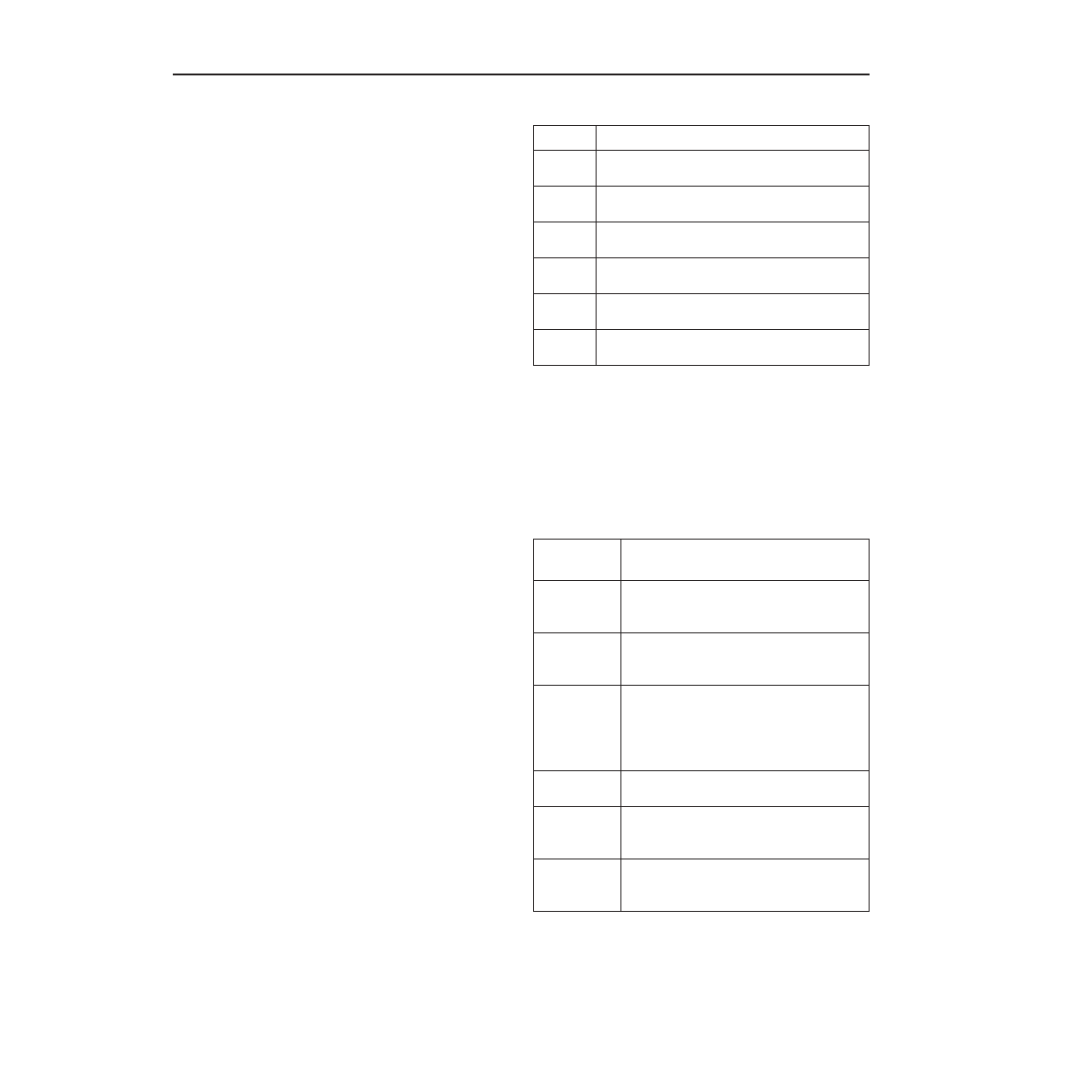
Table 15.
PIOLogicOptions
PIO Register Control Signals
The PIO latches/FFs have various clock, clock enable
(CE), local set/reset (LSR), and GSRN controls. Table
16 provides a summary of these control signals and
their effect on the PIO latches/FFs. Note that all control
signals are optionally invertible.
Table 16. PIO Register Control Signals
Option
Description
AND
OutputlogicalANDofsignalsonOUTDD
andclock.
NAND
OutputlogicalNANDofsignalsonOUTDD
andclock.
OR
OutputlogicalORofsignalsonOUTDD
andclock.
NOR
OutputlogicalNORofsignalsonOUTDD
andclock.
XOR
OutputlogicalXORofsignalsonOUTDD
andclock.
XNOR OutputlogicalXNORofsignalsonOUTDD
andclock.
Control
Signal
Effect/Functionality
EdgeClock
(ECLK)
Clocksinputfast-capturelatch;option-
allyclocksoutputFF,or
3-stateFF,orPIOshiftregisters.
System
Clock
(SCLK)
Clocksinputlatch/FF;optionallyclocks
outputFF,or3-stateFF,orPIOshift
registers.
Clock
Enable(CE)
Optionallyenables/disablesinputFF
(notavailableforinputlatchmode);
optionallyenables/disablesoutputFF;
separateCEinversioncapabilityfor
inputandoutput.
LocalSet/
Reset(LSR)
Optiontodisable;affectsinputlatch/FF,
outputFF,and3-stateFFifenabled.
GlobalSet/
Reset
(GSRN)
OptiontoenableordisableperPIO
afterinitialconfiguration.
Set/Reset
Mode
Theinputlatch/FF,outputFF,and3-
stateFFareindividuallysetorresetby
boththeLSRandGSRNinputs.
相关PDF资料 |
PDF描述 |
|---|---|
| OR4E041BM680-DB | FPGA, 1296 CLBS, 380000 GATES, PBGA680 |
| OR4E042BA352-DB | FPGA, 1296 CLBS, 380000 GATES, PBGA352 |
| OR4E042BM416-DB | FPGA, 1296 CLBS, 380000 GATES, PBGA416 |
| OR4E042BM680-DB | FPGA, 1296 CLBS, 380000 GATES, PBGA680 |
| OR4E043BA352-DB | FPGA, 1296 CLBS, 380000 GATES, PBGA352 |
相关代理商/技术参数 |
参数描述 |
|---|---|
| OR4E04-1BM416I | 功能描述:FPGA - 现场可编程门阵列 10368 LUT 466 I/O RoHS:否 制造商:Altera Corporation 系列:Cyclone V E 栅极数量: 逻辑块数量:943 内嵌式块RAM - EBR:1956 kbit 输入/输出端数量:128 最大工作频率:800 MHz 工作电源电压:1.1 V 最大工作温度:+ 70 C 安装风格:SMD/SMT 封装 / 箱体:FBGA-256 |
| OR4E04-1BM680C | 功能描述:FPGA - 现场可编程门阵列 10368 LUT 466 I/O RoHS:否 制造商:Altera Corporation 系列:Cyclone V E 栅极数量: 逻辑块数量:943 内嵌式块RAM - EBR:1956 kbit 输入/输出端数量:128 最大工作频率:800 MHz 工作电源电压:1.1 V 最大工作温度:+ 70 C 安装风格:SMD/SMT 封装 / 箱体:FBGA-256 |
| OR4E04-1BM680I | 功能描述:FPGA - 现场可编程门阵列 10368 LUT 466 I/O RoHS:否 制造商:Altera Corporation 系列:Cyclone V E 栅极数量: 逻辑块数量:943 内嵌式块RAM - EBR:1956 kbit 输入/输出端数量:128 最大工作频率:800 MHz 工作电源电压:1.1 V 最大工作温度:+ 70 C 安装风格:SMD/SMT 封装 / 箱体:FBGA-256 |
| OR4E04-2BA352C | 功能描述:FPGA - 现场可编程门阵列 10368 LUT 466 I/O RoHS:否 制造商:Altera Corporation 系列:Cyclone V E 栅极数量: 逻辑块数量:943 内嵌式块RAM - EBR:1956 kbit 输入/输出端数量:128 最大工作频率:800 MHz 工作电源电压:1.1 V 最大工作温度:+ 70 C 安装风格:SMD/SMT 封装 / 箱体:FBGA-256 |
| OR4E04-2BA352I | 功能描述:FPGA - 现场可编程门阵列 10368 LUT 466 I/O RoHS:否 制造商:Altera Corporation 系列:Cyclone V E 栅极数量: 逻辑块数量:943 内嵌式块RAM - EBR:1956 kbit 输入/输出端数量:128 最大工作频率:800 MHz 工作电源电压:1.1 V 最大工作温度:+ 70 C 安装风格:SMD/SMT 封装 / 箱体:FBGA-256 |
发布紧急采购,3分钟左右您将得到回复。