- 您现在的位置:买卖IC网 > PDF目录189449 > OR4E041BM416-DB (LATTICE SEMICONDUCTOR CORP) FPGA, 1296 CLBS, 380000 GATES, PBGA416 PDF资料下载
参数资料
| 型号: | OR4E041BM416-DB |
| 厂商: | LATTICE SEMICONDUCTOR CORP |
| 元件分类: | FPGA |
| 英文描述: | FPGA, 1296 CLBS, 380000 GATES, PBGA416 |
| 封装: | PLASTIC, FBGA-416 |
| 文件页数: | 60/151页 |
| 文件大小: | 2680K |
| 代理商: | OR4E041BM416-DB |
第1页第2页第3页第4页第5页第6页第7页第8页第9页第10页第11页第12页第13页第14页第15页第16页第17页第18页第19页第20页第21页第22页第23页第24页第25页第26页第27页第28页第29页第30页第31页第32页第33页第34页第35页第36页第37页第38页第39页第40页第41页第42页第43页第44页第45页第46页第47页第48页第49页第50页第51页第52页第53页第54页第55页第56页第57页第58页第59页当前第60页第61页第62页第63页第64页第65页第66页第67页第68页第69页第70页第71页第72页第73页第74页第75页第76页第77页第78页第79页第80页第81页第82页第83页第84页第85页第86页第87页第88页第89页第90页第91页第92页第93页第94页第95页第96页第97页第98页第99页第100页第101页第102页第103页第104页第105页第106页第107页第108页第109页第110页第111页第112页第113页第114页第115页第116页第117页第118页第119页第120页第121页第122页第123页第124页第125页第126页第127页第128页第129页第130页第131页第132页第133页第134页第135页第136页第137页第138页第139页第140页第141页第142页第143页第144页第145页第146页第147页第148页第149页第150页第151页
16
Lattice Semiconductor
Data Sheet
September, 2002
ORCA Series 4 FPGAs
Programmable Logic Cells (continued)
The ripple mode can be used in one of four submodes.
The rst of these is adder-subtractor submode. In
this submode, each LUT generates three separate out-
puts. One of the three outputs selects whether the
carry-in is to be propagated to the carry-out of the cur-
rent LUT or if the carry-out needs to be generated. If
the carry-out needs to be generated, this is provided by
the second LUT output. The result of this selection is
placed on the carry-out signal, which is connected to
the next LUT carry-in or the COUT/FCOUT signal, if it
is the last LUT (K7/K3). Both of these outputs can be
any equation created from KZ[1] and KZ[0], but in this
case, they have been set to the propagate and gener-
ate functions.
The third LUT output creates the result bit for each LUT
output connected to F[7:0]/F[3:0]. If an adder/subtrac-
tor is needed, the control signal to select addition or
subtraction is input on F5A/F5C inputs. These inputs
generate the controller input AS. When AS = 0 this
function performs the adder, A + B. When AS = 1 the
function performs the subtractor, A – B. The result bit is
created in one-half of the LUT from a single bit from
each input bus KZ[1:0], along with the ripple input bit.
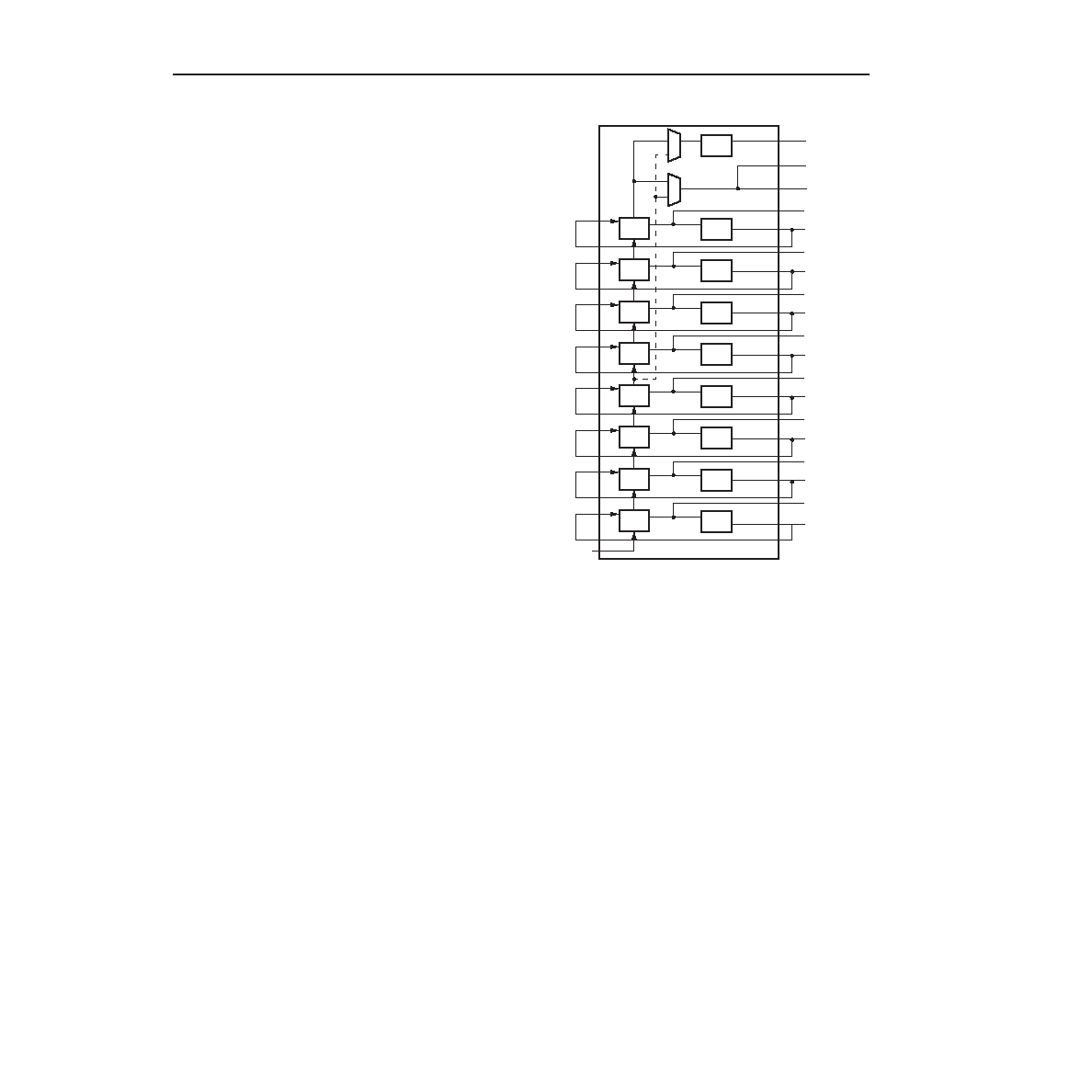
The second submode is the counter submode (see
Figure 10). The present count, which may be initialized
via the PFU DIN inputs to the latches/FFs, is supplied
to input KZ[0], and then output F[7:0]/F[3:0] will either
be incremented by one for an up counter or decre-
mented by one for a down counter. If an up/down
counter is needed, the control signal to select the direc-
tion (up or down) is input on F5A and F5C. When
F5[A:C], respectively per nibble, is a logic 1, this indi-
cates a down counter and a logic 0 indicates an up
counter.
5-5756(F)
Figure 10. Counter Submode
F7
K7[0]
K7
DQ
C
DQ
Q7
REGCOUT
COUT
F6
K6[0]
K6
DQ
Q6
F4
K4[0]
K4
DQ
Q4
F3
K3[0]
K3
DQ
Q3
F2
K2[0]
K2
DQ
Q2
F1
K1[0]
K1
DQ
Q1
F5
K5[0]
K5
DQ
Q5
F0
K0[0]
K0
DQ
Q0
CIN/FCIN
FCOUT
相关PDF资料 |
PDF描述 |
|---|---|
| OR4E041BM680-DB | FPGA, 1296 CLBS, 380000 GATES, PBGA680 |
| OR4E042BA352-DB | FPGA, 1296 CLBS, 380000 GATES, PBGA352 |
| OR4E042BM416-DB | FPGA, 1296 CLBS, 380000 GATES, PBGA416 |
| OR4E042BM680-DB | FPGA, 1296 CLBS, 380000 GATES, PBGA680 |
| OR4E043BA352-DB | FPGA, 1296 CLBS, 380000 GATES, PBGA352 |
相关代理商/技术参数 |
参数描述 |
|---|---|
| OR4E04-1BM416I | 功能描述:FPGA - 现场可编程门阵列 10368 LUT 466 I/O RoHS:否 制造商:Altera Corporation 系列:Cyclone V E 栅极数量: 逻辑块数量:943 内嵌式块RAM - EBR:1956 kbit 输入/输出端数量:128 最大工作频率:800 MHz 工作电源电压:1.1 V 最大工作温度:+ 70 C 安装风格:SMD/SMT 封装 / 箱体:FBGA-256 |
| OR4E04-1BM680C | 功能描述:FPGA - 现场可编程门阵列 10368 LUT 466 I/O RoHS:否 制造商:Altera Corporation 系列:Cyclone V E 栅极数量: 逻辑块数量:943 内嵌式块RAM - EBR:1956 kbit 输入/输出端数量:128 最大工作频率:800 MHz 工作电源电压:1.1 V 最大工作温度:+ 70 C 安装风格:SMD/SMT 封装 / 箱体:FBGA-256 |
| OR4E04-1BM680I | 功能描述:FPGA - 现场可编程门阵列 10368 LUT 466 I/O RoHS:否 制造商:Altera Corporation 系列:Cyclone V E 栅极数量: 逻辑块数量:943 内嵌式块RAM - EBR:1956 kbit 输入/输出端数量:128 最大工作频率:800 MHz 工作电源电压:1.1 V 最大工作温度:+ 70 C 安装风格:SMD/SMT 封装 / 箱体:FBGA-256 |
| OR4E04-2BA352C | 功能描述:FPGA - 现场可编程门阵列 10368 LUT 466 I/O RoHS:否 制造商:Altera Corporation 系列:Cyclone V E 栅极数量: 逻辑块数量:943 内嵌式块RAM - EBR:1956 kbit 输入/输出端数量:128 最大工作频率:800 MHz 工作电源电压:1.1 V 最大工作温度:+ 70 C 安装风格:SMD/SMT 封装 / 箱体:FBGA-256 |
| OR4E04-2BA352I | 功能描述:FPGA - 现场可编程门阵列 10368 LUT 466 I/O RoHS:否 制造商:Altera Corporation 系列:Cyclone V E 栅极数量: 逻辑块数量:943 内嵌式块RAM - EBR:1956 kbit 输入/输出端数量:128 最大工作频率:800 MHz 工作电源电压:1.1 V 最大工作温度:+ 70 C 安装风格:SMD/SMT 封装 / 箱体:FBGA-256 |
发布紧急采购,3分钟左右您将得到回复。