- 您现在的位置:买卖IC网 > PDF目录11732 > ORSO42G5-1BMN484I (Lattice Semiconductor Corporation)IC TRANCEIVERS FPSC 680FPGAM PDF资料下载
参数资料
| 型号: | ORSO42G5-1BMN484I |
| 厂商: | Lattice Semiconductor Corporation |
| 文件页数: | 100/153页 |
| 文件大小: | 0K |
| 描述: | IC TRANCEIVERS FPSC 680FPGAM |
| 产品变化通告: | Product Discontinuation 01/Aug/2011 |
| 标准包装: | 60 |
| 系列: | * |
第1页第2页第3页第4页第5页第6页第7页第8页第9页第10页第11页第12页第13页第14页第15页第16页第17页第18页第19页第20页第21页第22页第23页第24页第25页第26页第27页第28页第29页第30页第31页第32页第33页第34页第35页第36页第37页第38页第39页第40页第41页第42页第43页第44页第45页第46页第47页第48页第49页第50页第51页第52页第53页第54页第55页第56页第57页第58页第59页第60页第61页第62页第63页第64页第65页第66页第67页第68页第69页第70页第71页第72页第73页第74页第75页第76页第77页第78页第79页第80页第81页第82页第83页第84页第85页第86页第87页第88页第89页第90页第91页第92页第93页第94页第95页第96页第97页第98页第99页当前第100页第101页第102页第103页第104页第105页第106页第107页第108页第109页第110页第111页第112页第113页第114页第115页第116页第117页第118页第119页第120页第121页第122页第123页第124页第125页第126页第127页第128页第129页第130页第131页第132页第133页第134页第135页第136页第137页第138页第139页第140页第141页第142页第143页第144页第145页第146页第147页第148页第149页第150页第151页第152页第153页
Lattice Semiconductor
ORCA ORSO42G5 and ORSO82G5 Data Sheet
50
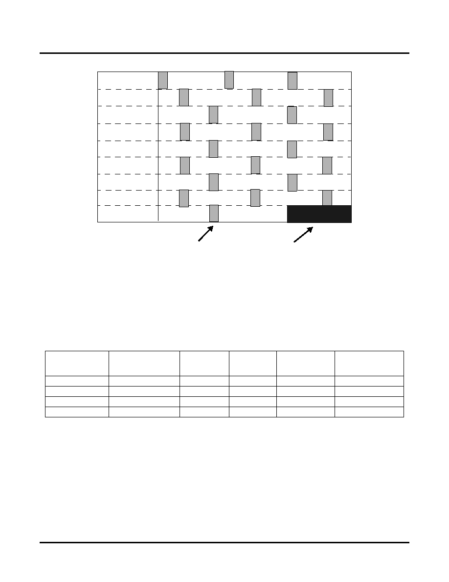
Figure 36. Cell Mapping in SONET Frame
The cells are placed in a SONET frame such that the rst cell starts at the rst SPE column of the rst row (145th
column. 144 columns are taken up by TOH). Subsequent cells are placed contiguously, skipping the Transport
OverHead (TOH) columns when appropriate.
The ORSO42G5 and ORSO82G5 supports four cell sizes with varying payloads. The total cell size sent across the
backplane is the combined size of the user cell payload (cell header and data), user BIP and the Link Header byte.
Table 9 indicates the cell sizes supported by the ORSO42G5 and ORSO82G5 within a STS-48c frame. Only one
cell size can be used at a time.
Table 9. ORSO42G5 and ORSO82G5 Supported Cell Sizes
A cell cannot span multiple SONET frames. This implies that there may be some cell sizes for which some bytes
will be unused at the end of a SPE. These are called pad bytes.
Each cell is preceded by a Link Header byte as shown in Figure 37. Table 10 denes the format of the Link Header.
The Link Header byte is useful for cell delineation when cell data are striped across multiple links. The Link Header
is inserted automatically in the transmit direction by the IPC block. The Link Header is checked in the receive direc-
tion and removed by the OPC before the cell is sent across the core/FPGA interface.
Total Cell Size
(Across B/P)
User Cell Payload
Size
(Header/Data)
Link Header
Byte
User BIP Field
Cells/Frame
Number of Pad
Bytes Per SPE
77
75
1
488
8
81
79
1
464
0
85
83
1
442
14
93
91
1
404
12
Note:
To calculate the number of cells per SPE:
[(87Rows/STS-1*9Columns/STS-1)octets/(STS-1 SPE)] * 48 STS-1 = 37584 octets
337584 / TOTAL CELL SIZE = # of cells per SPE.
TO
H
BYTES
A1 A2 J0
Cell 0
Cell 1
Cell 2 (etc.)
Link Header byte
Pad bytes
BYTES
CELL
P
A
YLO
AD
相关PDF资料 |
PDF描述 |
|---|---|
| V300A36E500BG2 | CONVERTER MOD DC/DC 36V 500W |
| VE-B00-IX-F1 | CONVERTER MOD DC/DC 5V 75W |
| ORSO42G5-2BMN484I | IC TRANCEIVERS FPSC 680FPGAM |
| ORSO42G5-1BMN484C | IC TRANCEIVERS FPSC 680FPGAM |
| VE-B03-IX-F1 | CONVERTER MOD DC/DC 24V 75W |
相关代理商/技术参数 |
参数描述 |
|---|---|
| ORSO42G5-2BM484C | 功能描述:FPGA - 现场可编程门阵列 10368 LUT 204 I/O RoHS:否 制造商:Altera Corporation 系列:Cyclone V E 栅极数量: 逻辑块数量:943 内嵌式块RAM - EBR:1956 kbit 输入/输出端数量:128 最大工作频率:800 MHz 工作电源电压:1.1 V 最大工作温度:+ 70 C 安装风格:SMD/SMT 封装 / 箱体:FBGA-256 |
| ORSO42G5-2BM484I | 功能描述:FPGA - 现场可编程门阵列 10368 LUT 204 I/O RoHS:否 制造商:Altera Corporation 系列:Cyclone V E 栅极数量: 逻辑块数量:943 内嵌式块RAM - EBR:1956 kbit 输入/输出端数量:128 最大工作频率:800 MHz 工作电源电压:1.1 V 最大工作温度:+ 70 C 安装风格:SMD/SMT 封装 / 箱体:FBGA-256 |
| ORSO42G5-2BMN484C | 功能描述:FPGA - 现场可编程门阵列 10368 LUT 204 I/O RoHS:否 制造商:Altera Corporation 系列:Cyclone V E 栅极数量: 逻辑块数量:943 内嵌式块RAM - EBR:1956 kbit 输入/输出端数量:128 最大工作频率:800 MHz 工作电源电压:1.1 V 最大工作温度:+ 70 C 安装风格:SMD/SMT 封装 / 箱体:FBGA-256 |
| ORSO42G5-2BMN484I | 功能描述:FPGA - 现场可编程门阵列 10368 LUT 204 I/O RoHS:否 制造商:Altera Corporation 系列:Cyclone V E 栅极数量: 逻辑块数量:943 内嵌式块RAM - EBR:1956 kbit 输入/输出端数量:128 最大工作频率:800 MHz 工作电源电压:1.1 V 最大工作温度:+ 70 C 安装风格:SMD/SMT 封装 / 箱体:FBGA-256 |
| ORSO42G5-3BM484C | 功能描述:FPGA - 现场可编程门阵列 10368 LUT 204 I/O RoHS:否 制造商:Altera Corporation 系列:Cyclone V E 栅极数量: 逻辑块数量:943 内嵌式块RAM - EBR:1956 kbit 输入/输出端数量:128 最大工作频率:800 MHz 工作电源电压:1.1 V 最大工作温度:+ 70 C 安装风格:SMD/SMT 封装 / 箱体:FBGA-256 |
发布紧急采购,3分钟左右您将得到回复。